EDS Measurement of Palladium (Pd) - Practical Electron Microscopy and Database - - An Online Book - |
|||||||||||||||||||||||
| Microanalysis | EM Book https://www.globalsino.com/EM/ | |||||||||||||||||||||||
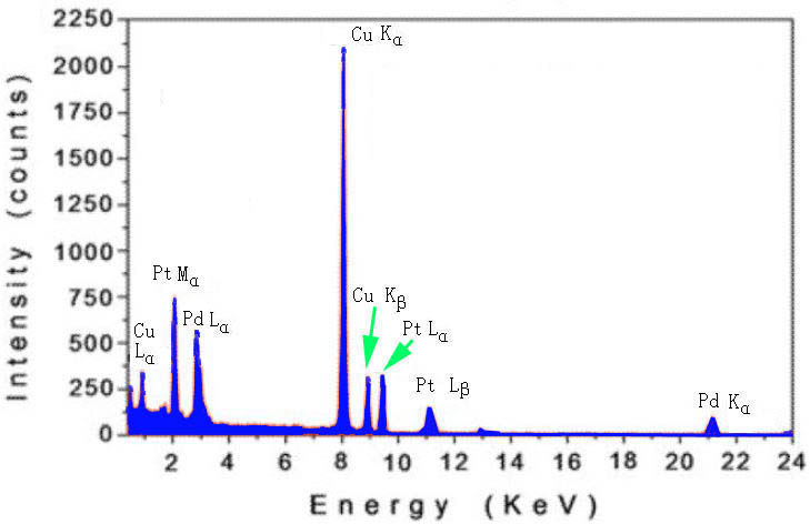
Table 1394 lists the comparison of EELS and EDS measurements on thin TEM samples with Pd elements. The comparisons are based on the same data acquisition condition, consequently the same electron dose used.
The EDS spectrum in Figure 1394 was taken from a nanoparticle (with Pt and Pd compositions of 50 at.% : 50 at.%) on holey carbon (C) film supported by a copper TEM grid. The copper signal in the spectrum was from the Cu grid (see page4638).
|
|
||||||||||||||||||||||