=================================================================================
In integrated circuits (ICs), conductive lines provide electrical interconnection among different parts of the ICs, devices, and the outside. The main applications of metallization are classified by gate, contact, and interconnection. Polysilicon and silicides are commonly applied as gates and interconnects in MOS devices. Copper, tungsten, silver, titanium, platinum, gold, and palladium are used as these types of contacts, connections, and/or interconnection to external components. Aluminum films are frequently used as interconnections in semiconductor devices and integrated circuits.
Table 2035a. Properties of some metals commonly used in ICs.
Property\metal |
Cu |
Al |
W |
Au |
Ag |
Resistivity (10-6 Ω•cm) |
1.67 |
2.7 - 3.0 |
5.65 |
2.35 |
1.59 |
Melting point (°C) |
1085 |
660 |
3387 |
1064 |
962 |
Thermal conductivity (Wcm-1) |
3.98 |
2.358 |
1.74 |
3.15 |
4.25 |
Thermal stress per degree for
films on silicon (107 dyn cm-2 °C-1) |
2.5 |
2.1 |
0.8 |
1.2 |
1.9 |
Coefficient of thermal expansion (CTE)
(10-6 °C-1) |
17 |
23.5 |
4.5 |
14.2 |
19.1 |
Youngs modulus (x10-11 dyn cm-2) |
12.98 |
7.06 |
41.1 |
7.85 |
8.27 |
Corrosion in air |
Poor |
Good |
Good |
Excellent |
Poor |
Specific heat capacity(Jkg-1K-1) |
38 |
917 |
138 |
132 |
234 |
Adhesion to SiO2 |
Poor |
Good |
Poor |
Poor |
Poor |
Aluminum has most of the desired characteristics listed on page2039, but it suffers from a low melting point, spiking shorts, and electromigration.
Table 2035b. Metallization selections in ICs.
Application |
Selection |
Gates, interconnection, and
contacts |
Polysilicon, refractory metal silicides (e.g. MoSix, TaSix, WSix, and TiSix), nitrides,aluminum, copper, and/or refractory metals. |
Diffusion barrier layer |
Ti, TiN, Ta, TaN, Ti-W alloy, and/or silicides |
Top level |
Aluminum, and/or copper |
Metallization
on silicon |
Silicides, tungsten, aluminum, and/or copper |
Figure 2035 shows the historical view of Ohmic contact developments in Si(silicon)-based ICs. Ideally, Al (aluminum) would be deposited directly onto Si with perfect interfaces between Al and Si as shown in Figure 2035 (a). Unfortunately, the Si migrates into the Al, resulting in voids (pits) formed in the Si as shown in Figure 2035 (b). Void formation can happen, for instance, when annealing Al on Si at 450 0C. The Al can subsequently migrate into the formed voids, inducing spiking as shown in Figure 2035 (c). The big spike leads to junction shorts between n+ and p layers. Because the solubility of Si in Al is small (e.g. 0. 5 wt% at 450 °C), low Si doping in Al (1 to 3 wt% Si) suppresses spike formation significantly. However, other problems can occur subsequently, for instance, Al-doped p+ Si can precipitate out or p+ Si epitaxial layer can be formed between the original Si surface and the Al film as shown in Figure 2035 (d). Note that here Al is a p-type of dopants in Si. Furthermore, a challenge is that the formation probability of such epitaxial films is higher for (100)- than for (111)-oriented Si substrates. This can be more severe problem when the contact is scaled further and thus it only contains one or few grains.
Silicides were introduced to solve the precipitation problem. As shown in Figure 2035 (e), a silicide is formed by depositing a metal onto Si, followed by heating the sample. Here, the Al does not have to be doped with Si. However, the Al above the silicide can still migrate through the silicide along the grain boundaries of the silicide, resulting in formation of Al/Si contacts as shown in Figure 2035 (f). This migration can be enhanced by the high compressive stress in the Al induced by its high CTE than that of Si (CTEAl>> CTESi) at high temperatures. Recently, barrier layers are introduced to address the migration problem as shown in Figure 2035 (g). These barrier layers have the properties of low contact resistance, and good chemical, electrical, and mechanical stabilities.
If the contact is fabricated on p-type silicon as shown in Figure 2035 (h), the silicon migration, formation of small voids, and weak Al penetration probably will not cause significant performance problems in the IC.
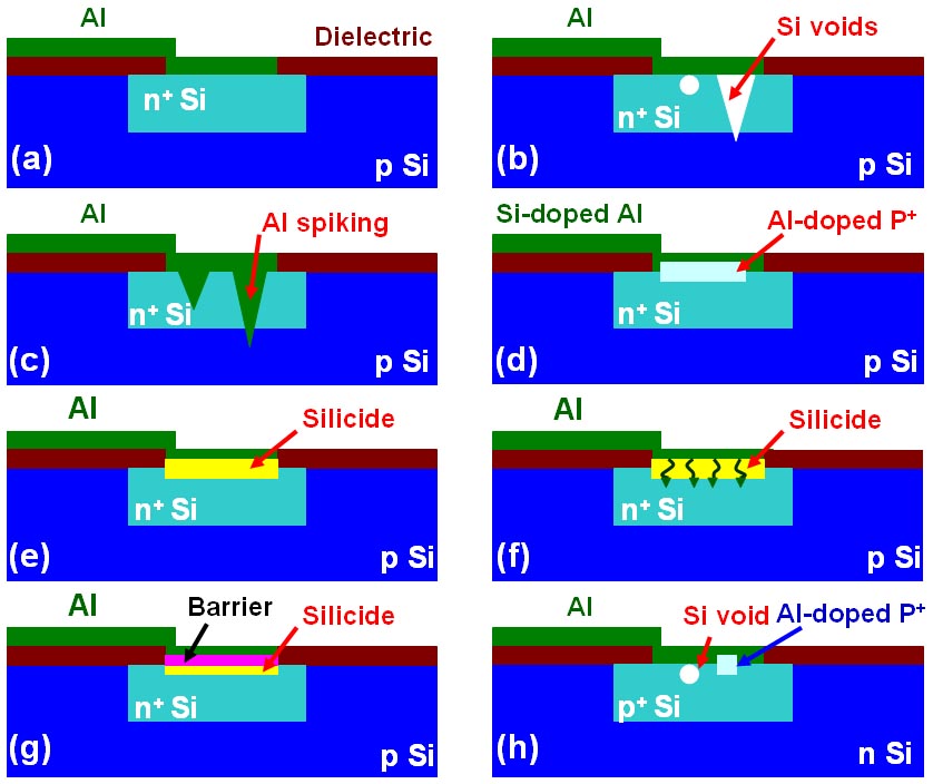
Figure 2035. Historical view of Ohmic contact developments in Si-based ICs: (a) Al deposited directly onto Si; (b) Voids formed in Si; (c) Al spiking; (d) p+ Si formation; (e) Silicides; (f) Formation of Al/Si contacts; (g) Barrier layer/silicide; and (h) Contact on p-type silicon.
Electromigration in Al can occur under the influence of an electric field in ICs. The electromigration induces voids, resulting in discontinuities, in the metallization runners, that causes circuit opening and/or pileups that can cause short circuit failure to adjacent conductors. The electromigration resistance of Al can be increased by alloying with copper at low concentrations, e.g. ~ 0.5%.
|