|
This book (Practical Electron Microscopy and Database) is a reference for TEM and SEM students, operators, engineers, technicians, managers, and researchers.
|
=================================================================================
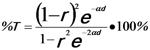
In many cases of TLS (thermal laser stimulation) measurements, wafer back grinding is needed because thinning of the wafers improves the signal strength. Figure 2809 shows the percent transmission as a function of wavelength and p-doping concentration for 625 pm of Si [1]. Heavier doping increases laser absorption and thus reduces transmission. The percent transmission of infrared wavelengths is given by [1],
 ----------------------------- [2809] ----------------------------- [2809]
where,
%T -- The percent transmission,
r -- The reflection coefficient,
α -- The absorption coefficient,
d -- The thickness of Si wafer.
As indicated in Equation 2809, decreasing the thickness can dramatically increase the %T and therefore the TLS signal.
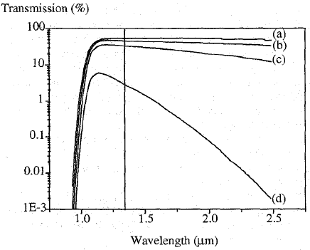
Figure 2809. Percent transmission of laser intensity through p-doped Si in 625 pm thickness and having doping concentrations of (a) 1.5 x 10¹⁶, (b) 3.3 x 10¹⁷, (c) 1.2 x 10¹⁸, and (d) 7.3 x 1018 cm-3. The 1340 nm wavelength is marked by a vertical line. [2]
[1] S. E. Aw, H. S. Tan, and C. K. Qng, “Optical Absorption Measurements of Band-gap Shrinkage in Moderately and Heavily Doped Silicon”, J. Phys.: Condens. Mutter, 3, 1991, pp. 8213-8223.
[2] Cole, EI; Tangyunyong, P; Barton, DL, Backside localization of open and shorted IC interconnections, 36th Annual IEEE International Reliability Physics Symposium, (1998). DOI: 10.1109/RELPHY.1998.670462.
|