=================================================================================
The people now believe that the scaling limit to Moore’s law is lithography because of the need for shorter wavelengths of light to pattern the smaller feature sizes. Therefore, materials are now a key constraint in silicon technology. For example, the current density of conductors in ICs can be increased by using copper instead of aluminium. The RC time delays can be minimized using materials with lower dielectric constants instead of SiO2. Leakage in MOS structures can be minimized using materials, with high dielectric constants, between the gate and the silicon channel in FET in stead of SiO2.
The cross-sectional STEM image of a MOS transistor in Figure 2916 presents nickel silicide penetration into junction due to the abnormal growth of the Ni silicide. This Ni silicide penetration induced junction leakage-current in the MOS transistor. With plasmon loss in EELS, Kudo et al. [1] suggested that the Ni silicide in the abnormal growth area was nickel-disilicide (NiSi2). Starting from the understanding of the various mechanisms of crystalline growth, the abnormal growth can suppressed by controlling the crystal microstructure of the Si substrate, for instance, by using Si ion implantation [2], nitrogen ion implantation [3], the optimization of the conditions of gate sidewall etching [1], or the choice of the substrate direction [4].
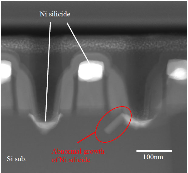
Figure 2916. Nickel silicide penetration into junction of a MOS transistor due to the abnormal growth of the Ni silicide. [1]
[1] S. Kudo, Y. Hirose, N. Hashikawa, T. Yamaguchi, K. Kashihara, K. Maekawa, K. Asai, N. Murata, K. Asayama and E. Murakami, Analysis of Ni Silicide Abnormal Growth Mechanism Using Advanced TEM Techniques, IEEE International Reliability Physics Symposium, 2008. IRPS (2008) 10074334.
[2] T. Yamaguchi et al., “Suppression of Anomalous Gate Edge
Leakage Current by Control of Ni Silicidation Region using Si
Ion Implantation Technique”, IEDM Tech. Dig., 2006, pp855-858.
[3] K. Kashihara et al., “Improvement of thermal stability of
nickel silicide using N2 ion implantation prior to nickel film
deposition”, Proceedings of The 6th International Workshop
on Junction Technology, 2006, pp176-179.
[4] T. Yamaguchi et al., “A Novel Low Leakage-Current Ni
Silicide Process in nMOSFETs on Si (110) Substrate”, IEDM
Tech. Dig., 2007, pp139-142.
|