|
|
Extra Electron Diffraction Spots from
Perovskite Crystalline Structures
- Practical Electron Microscopy and Database -
- An Online Book -
|
|
https://www.globalsino.com/EM/
|
|
This book (Practical Electron Microscopy and Database) is a reference for TEM and SEM students, operators, engineers, technicians, managers, and researchers.
|
=================================================================================
The double perovskite crystalline structures can be described by an F-centred 2a0 x 2a0 x 2a0 superlattice (where a0 is the lattice parameter of the ideal perovskite structures). As results, extra diffraction spots present besides the "standard" electron diffraction spots from the ideal perovskite crystalline structures. As an example, Figure 3522 (a) shows the dark field image revealing B-site ordered domains (bright areas) in PMN materials and (b) presents such extra diffraction spots as well as the standard diffraction spots in the selected area diffraction pattern from the <l 1 0> zone axis of the area in Figure 3522 (a).
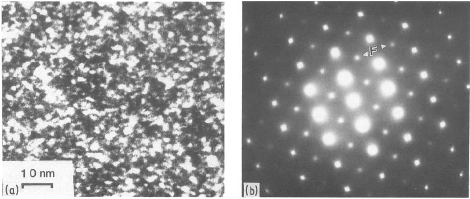
Figure 3522. (a) The dark field image revealing B-site ordered domains (bright areas) in
PMN materials and (b) The extra diffraction spots as well as the standard diffraction
spots from the <l 1 0> zone axis of the area in figure (a). [1]
[1] A. D. Hilton, D. J. Barber, C. A. Randall, and T. R. Shrout, Journal of Materials Science, 25, 3461(1990).
|
=================================================================================
The book author (Dr. Liao) welcomes your comments, suggestions, and corrections, please click here for submission. You can click How to Cite This Book to cite this book. If you let Dr. Liao know once you have cited this book, the brief information of your publication will appear on the “Times Cited” page. This appearance can help advertise your publication.
|
|