=================================================================================
Assuming the thickness of TEM samples is uniform, the contrast interpretation of HAADF STEM images will be much easier. For instance, Figure 4486a shows an image obtained from a structure with multilayers with SrRuO3 and SrTiO3 materials. In this image, the intensity scales with the atomic number Z of the compound and therefore, the bright layers correspond to SrRuO3, whereas the darker layers consist of SrTiO3. By changing a line (not shown) plot to a rectangle plot in Digital Micrograph (in case Gatan interface is used), the intensity profiles are made in which the peaks correspond to the SrRuO3 layers in Figure 4486a (B). The background intensity (indicated by the red line) is an indication of the sample thickness, suggesting the sample thickness on the right-hand side is slightly thinner. Note that the reason why a rectangle plot can be used instead of a line plot is that the materials in each material layer are identical, meaning either SrRuO3 or SrTiO3. However, the intensity profile in Figure 4486a (B) will be noisier if a line plot is used.
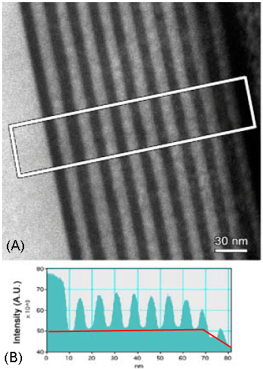
Figure 4486a. HAADF-STEM images of a multilayer sample, obtained
along the direction indicated by the white rectangle (adapted from [1]).
However, in many cases, HAADF images not only present Z-contrast but also include other contrasts, which can even result in contrast reversal. For instance, Figure 4486b shows the double perovskite-rocksalt oxide La2CuSnO6 (LCSO) with Cu2+ and Sn4+ ions determined by X-ray analysis. The La–La distance around the Cu ion is slightly shorter than that around the Sn ion, because the CuO6 octahedrons are slightly distorted by the Jahn–Teller effect. The alternation of CuO6 and SnO6 octahedral layers and the buckling of the CuO2 and SnO2 sheets induce a monoclinic superstructure with the lattice parameters of a = 0.8510, b = 0.7815, c = 0.7817 nm (corresponding to 2a0 x 2a0 x 2a0), and β = 91.151°. Note there are four non-equivalent La atoms with different atomic coordinates and Debye–Waller factors (MLa1 = 0.0056 nm2, MLa2 = 0.005 nm2, MLa3 = 0.0042 nm2, and MLa4 = 0.0081 nm2) in a unit cell [2].
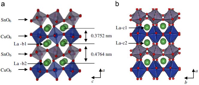
Figure 4486b. The double perovskite-rocksalt oxides La2CuSnO6 (LCSO) determined by X-ray analysis: (a) b-axis and (b) c-axis projections. [3]
Figure 4486c shows HAADF-STEM images of LCSO along the b- and c-axis projections, respectively. Table 4486 lists the factors affecting the HAADF contrast of the atoms. A large Debye–Waller factor reduces the depth of atomic potentials, resulting in broadening of the atomic image in HAADF [4]. Furthermore, this effect may lead to decrease in the high-angle scattering probability.
Even though the atomic number of La is larger than that of Sn, Haruta et al. [3] concluded that in the case of b-axis projection, the Sn columns are brighter than the La columns because of the channeling effect and the difference of Debye–Waller factors between the Sn and La atoms, while in the case of c-axis projection, the intensity of the Sn column appears brighter than that of the La columns only because of the effect of Debye–Waller factors.
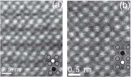
Figure 4486c. HAADF-STEM images of LCSO along the b- and c-axis projections, respectively. The contrasts in the circles represent the contrasts of the relevant atoms in the HAADF images. Adapted from [3]
Table 4486. Factors affecting the HAADF contrast of the atoms.
| Column |
Experimental
ADF contrast |
Atomic number |
Debye–Waller factors (nm2) of atoms in one unit cell |
Channeling effect |
| Location 1 |
Location 2 |
Location 3 |
Location 4 |
| Sn |
Brighter |
Smaller (Z=50) |
0.0031 |
0.0024 |
|
|
Significant |
| La |
Darker |
Larger (Z=57) |
0.0056 |
0.005 |
0.0042 |
0.0081 |
Significant |
The probe forming aperture in STEM is often compared to the objective aperture in parallel beam illumination in CTEM. The effect of aperture size on the CTF for HAADF STEM imaging is a much more complex issue. The point spread function is proportional to the square of the probe wavefunction and not the wavefunction itself (as in Bright field CTEM). The response to increasing the aperture size is non-linear and affects all spatial frequencies, not just the highest. The phase errors at large angles to the optic axis essentially are mixed in to the lower frequencies, degrading both contrast and image localization.
Although the HAADF STEM imaging offers an excellent alternative due to its Z-contrast, unwanted diffraction contrast in some degree, depending on the crystalline structure and elements in the specimen, still presents in general and affects the purity of Z-contrast.
For many complex compounds, one need to carefully select the observation direction for HAADF-STEM imaging in order to correctly analyze the Z-contrast of different elements with closer atomic numbers. In such cases, they need to first study the crystalline structure with simulators to figure out the crystal orientation in which each atomic column contains a single type of elements only. On the other hand, the number of atoms in a single atomic column may also need to be taken into account.
Figure 4486d shows the integrated ADF-STEM intensities versus strain amplitude of crystalline silicon (Si) over LAADF and the HAADF detectors. The LAADF signal increases when a strain field is introduced in LAADF image for thick TEM samples, while the HAADF signal stays essentially constant as strain amplitude increases.
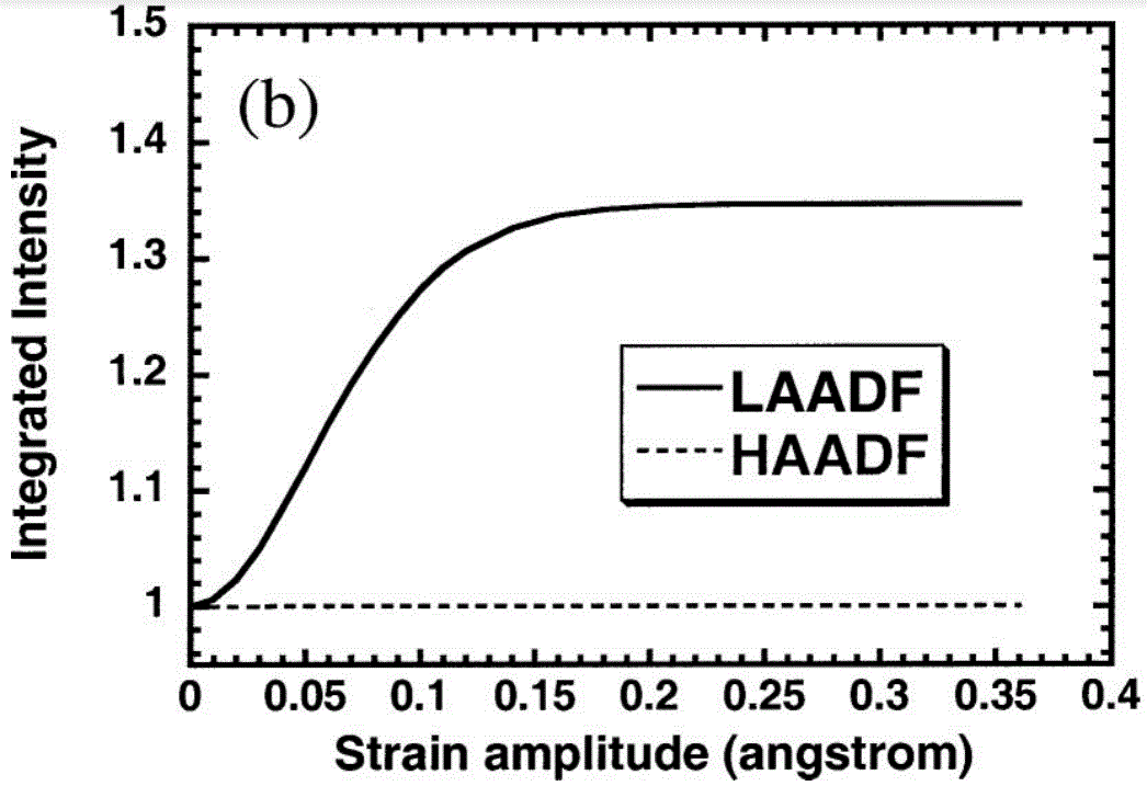
| Figure 4486d. Integrated ADF-STEM intensities versus strain amplitude over LAADF and the HAADF detectors, respectively. [5] |
[1] High-Quality Sample Preparation by Low kV FIB Thinning for Analytical TEM Measurements, Sara Bals, Wim Tirry, Remco Geurts, Zhiqing Yang, and Dominique Schryvers, Microsc. Microanal. 13, 80–86, (2007).
[2] M.T. Anderson, K.R. Poeppelmeier, Chem. Mater. 3 (1991) 476.
[3] M. Haruta, H. Kurata, H. Komatsu, Y. Shimakawa, S. Isoda, Effects of electron channeling in HAADF-STEM intensity in La2CuSnO6, Ultramicroscopy 109 (2009) 361–367.
[4] G.R. Anstis, D.Q. Cai, D.J.H. Cockayne, Ultramicroscopy 94 (2003) 309.
[5] Zhiheng Yu, David A. Muller, and John Silcox, Study of strain fields at a-Si/c-Si interface, J. Appl. Phys. 95, 3362 (2004).
|