=================================================================================
A direct and accurate measure of the TEM specimen thickness is essential for many aspects of TEM analyses, such as correction of X-ray intensities for absorption within the
specimen and for determination of actual sizes of two-dimensional (2-D)-projected features.
Specimen thickness may be determined by a variety of methods in TEM like projected width of
inclined stacking faults and EELS spectra. The popular and most accurate
technique for the measurement of the thickness of
crystalline specimens is convergent electron beam diffraction (CBED). The CBED method is based on the variation of the intensity of the diffracted beam with thickness known
as ‘Pendellösung’ fringes. For this case,
the specimen should be thicker than one extinction distance.
However, in practice, the CBED diffraction disks contain no contrast detail if a very thin region of a specimen (<0.1 µm) is under the electron beam. Diffraction from crystals in thickness of 0.1 - 0.5 µm does exhibit intensity variations, within the disks, which are caused by dynamical diffraction effect.
For CBED, the Bragg spots are extended to disks. CBED patterns contain Pendellösung fringes representing dynamical phenomenon. These fringes give information about the TEM specimen thickness and the real and imaginary Fourier coefficients, Vg and V’g, of the potential of the crystal lattice.
When exactly in a zone axis, the transmitted undiffracted
beam (000)-disc usually contains concentric diffuse fringes known as Kossel-Möllenstedt
(K-M) fringes. The number of the fringes increases by one every time the
thickness increases by one extinction distance. Thickness measurements
however are not made under zone-axis conditions but under two-beam
conditions with only one strongly excited (hkl)-reflection. Now the CBED discs
will contain parallel instead of concentric intensity oscillations. The central
bright fringe is in the exact Bragg condition. The fringe-spacing corresponds to
angles Δθi and from this spacing the deviation si for the ith-fringe can be
determined according to,
 ----------------------------------------- [4622a] ----------------------------------------- [4622a]
where,
λ -- The wavelength of the incident electrons
θB -- The Bragg angle for
the diffracting (hkl)-plane
d -- The (hkl)-interplanar spacing
The variation in s causes intensity oscillation across the disk. For instance, the intensity of a diffracted beam, Ig(s), is the function of an effective deviation parameter, seff:
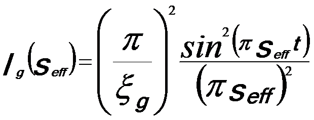 ---------------------------- [4622b]
where ξg is the extinction distance for the diffraction g. seff is given by,
 ----------------------------
[4622c] ----------------------------
[4622c]
Figure 4622a shows the calculated intensity profile of Ig as a function of s and 2θB (the separation of the (000)- and (hkl)-disks). The profile in Figure 4622a (a) is also called rocking curve.
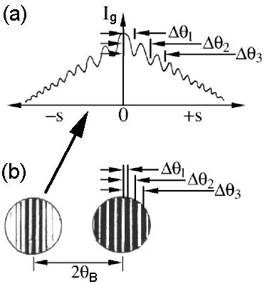
Figure 4622a. (a) The calculated intensity profile of Ig as a function of s (equals to an intensity trace taken across the g disk), and (b) The separation (2θB) of the (000)- and (hkl)-discs under two-beam
conditions
If the extinction distance ξg is known,
the foil thickness t can be determined according to,
 ----------------------------------------- [4622d] ----------------------------------------- [4622d]
where,
nk -- An integer.
These integers are assigned to the fringes, starting
with n = 1 for the first fringe, so that the thickness t can be determined
accurately. When this is not possible, the sample thickness may be larger
than one extinction distance and n = 2 should be assigned to the first fringe.
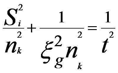
By plotting (si/nk)2 versus (1/nk)2 following Equation 4622d with the format in Table 4622, the specimen thickness is given by the
intercept of the resulting straight line with the (si/nk)2 -axis as shown in Figure 4622b.
Table 4622. Format to plot (si/nk)2 versus (1/nk)2.
| Δθ |
si |
n |
(si/nk)2 |
(1/nk)2 |
| Δθ1 |
|
n1 =1,2,3, ... |
|
|
| Δθ2 |
|
n1+1 |
|
|
| Δθ3 |
|
n1+2 |
|
|
| Δθ4 |
|
n1+3 |
|
|
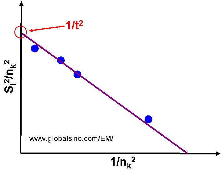
Figure 4622b. Example of plot of (si/nk)2 versus (1/nk)2.
Kelly et al. first proposed the thickness measurement technique using CBED [3] and then, Allen [6] had investigated the application and limitations of the technique. It has been easily to obtain a measurement accuracy of ±5% in metallic systems. Today this method has been widely used by many material
scientists as this offers accuracy better than 2% [1 - 5]. Furthermore, it should be mentioned that this technique has very limited applications to some materials such as most mineral specimens because of their large lattice parameters. It is difficult to obtain diffraction disks and true 'two-beam' kinematic conditions from the small reciprocal lattice dimensions of the large lattice parameters. In thickness measurements based on CBED, the diffraction disk should be large enough to contain at least three fringes.
Note that the thickness obtained by CBED includes only the thickness of crystalline materials so that it does not involve the amorphous layer on the TEM film. For instance, the amorphous layer generated by FIB damage is not included.
[1] Liao, Y., Degorce, J.-Y., Belisle, J., Meunier, M. (2006). 2D dopant determination in laser-diffused Si resistors using dopant-selective etching. Journal of the Electrochemical Society, 153(1), p. 16-22.
[2] Egerton R F 1986 Electron energy loss spectroscopy in the electron microscope (NewYork: Plenum)
[3] Kelly P M, Jostons A, Blake R G, Napier J G 1975 J. Appl. Phys. 62: 419
[4] Spence J C H, Zuo J M 1992 Electron microdiffraction (NewYork: Plenum)
[5] P. B. Hirsch, A. Howie, R. B. Nicholsen, D. W. Pashley
and M. J. Whelm, Electron Microscopy of Thin Crystals,
Butterworths, Washington 1965, pp. 179, 341.
[6] Allen, S. M. (1981) Phil. Maff. A43, 325.
|