=================================================================================
The spatial resolution of EFTEM is governed by several factors. The most important factors are the effect of delocalization of the inelastic scattering [1 - 3], the chromatic aberration of the objective lens, and the diffraction limit due to the objective aperture. For instance, if the EFTEM image is collected without
an objective aperture, the energy resolution is not compromised but spatial resolution is
poor. If it is done in diffraction mode and the collection angle (β) is controled by the entrance aperture, a large aperture (high
intensity, high β) will lower the spatial resolution and vice
versa.
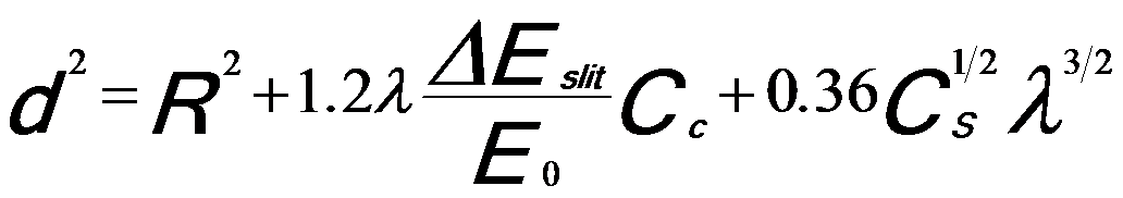
The resolution limits of inelastically filtered images in EFTEM have been theoretically predicted by several researchers [4 - 6]. The spatial resolution of the inelastic images can be expressed by the following equation,
 ---------- [4971a] ---------- [4971a]
where,
R -- An inelastic scattering delocalization factor;
ΔEslit -- The energy slit width;
E0 -- Eenergy of incident electron beam.
The second term in Equation 4971a is related to a beam broadening factor due to chromatic aberration (Cc) of the objective lens because of the finite width of the energy-selecting slit. The last term is related to spherical aberration (Cs) of the objective lens.
The inelastic delocalization factor R can be estimated by the root mean square impact parameter drms proposed by Pennycook[1].
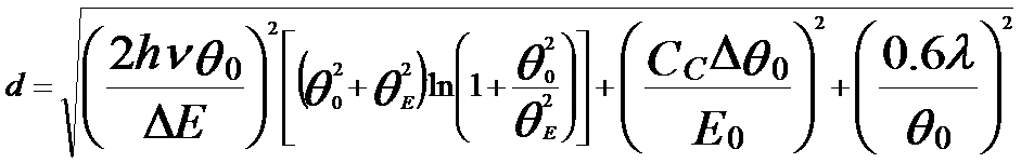
Therefore, the resolution can be given in a different way, [5]
 -- [4971b] -- [4971b]
where,
h -- Planck-constant
ν -- Wave-frequency
ΔE -- Energy loss
CC -- Chromatic aberration coefficients
λ -- wavelength of incident electron beam
θo -- Semiangle
due to the objective aperture size, namely objective lens collection semi-angle
θE -- The characteristic scattering semiangle, given by,
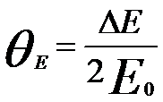 --------------------------------------------[4971c] --------------------------------------------[4971c]
 --------------------------------------------[4971d] --------------------------------------------[4971d]
drms -- the root mean square impact parameter.
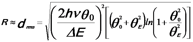
A simple estimation of the EFTEM spatial resolution affected by chromatic broadening is given by,
 ----------------------- (4971e) ----------------------- (4971e)
where,
β -- The collection angle.
We also can obtain the defocus, Δf, of the electrons that differ by an energy ΔE from those in focus,
 ----------------------- (4971f) ----------------------- (4971f)
For instance, the chromatic broadening (Δdc) is about 2.5 nm at β = 10 mrad, Cc = 1 mm, ΔE = 50 eV, and E0 = 200 keV. For thick specimens (with multiple scattering) the calculation in Equation 4971e predicts the Cc-effect on the spatial resolution well, while for a thin specimen the characteristic inelastic scattering angle is much smaller, given by,
θe = γΔE/2E0 ----------------------- (4971g)
where,
γ -- The relativistic correction
factor (=(E0+mec2)/(E0+2mec2), e.g. =0.61 for 300 kV).
θe is normally ≤0.6 mrad. Substituting θe for β in Equation 4971e, we can know that Δdc is normally ≤ 0.2 nm for most microscope configurations.
Most parameters in Equation 4971b are either fixed in microscopes, like CC, or should not be lowered such as E0 (or λ) in order to obtain a good resolution. One variable is θ0 as mentioned above. Although the chromatic error is decreased for small θ0, the aperture size (and thus θ0) has
to be compromised against the loss of useful signal. The chromatic errors due to the objective lens also increase with the width of the energy window Δ, while the amount of delocalization depends on the mean core-loss filtering energy (e.g. in three-window case as shown in Figure 4971a) and decreases for higher energy losses ΔE.
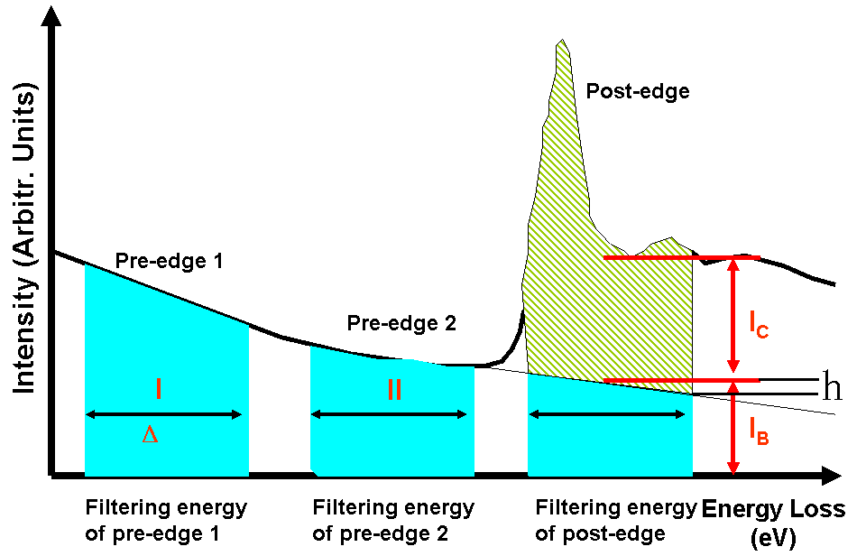
Figure 4971a. Schematic of three-window methods for EFTEM elemental mapping and EELS elemental quantification.
Figure 4971b shows the schematic illustration of the broadening of electron beam within a thin specimen and of generations of EDS, EELS and AES signals. This beam broadening affects the spatial resolution of EDS significantly, but does not affect those of EELS and AES too much. d, R and Rmax are the spot size , the average diameter, and the maximum diameter of the electron beam within the specimen, respecitively. α and β are convergence semiangle of the electron beam and the collection semiangle of EELS/EFTEM. The angle-limiting aperture can be the objective aperture of TEM/STEM system or the entrance aperture of the EELS system, which is smaller and dominates the beam intensity arriving at the camera.
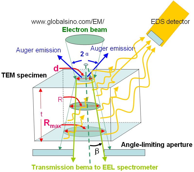
Figure 4971b. Schematic illustration of the broadening of electron beam
within a thin specimen and of generations of EDS, EELS and AES signals.
Figure 4971c shows the theoretical plots of the spatial resolution of the energy-filtered images as a function of the loss energy for a 300 kV TEM [7]. In the modeling, the energy slit width used was 20 eV, the characteristic scattering angle was considered to be 0.1 rad (~5.7°), and the spherical and chromatic aberrations are 0.6 and 1.5 mm, respectively. In conclusion, the figure indicates the spatial resolution is dominated by the inelastic delocalization factor (R) at the energy losses lower than ~100 eV, while at an energy losses higher than ~100 eV, the spatial resolution is mainly affected by both the chromatic broadening (Dcc) and the spherical broadening (Dcs).
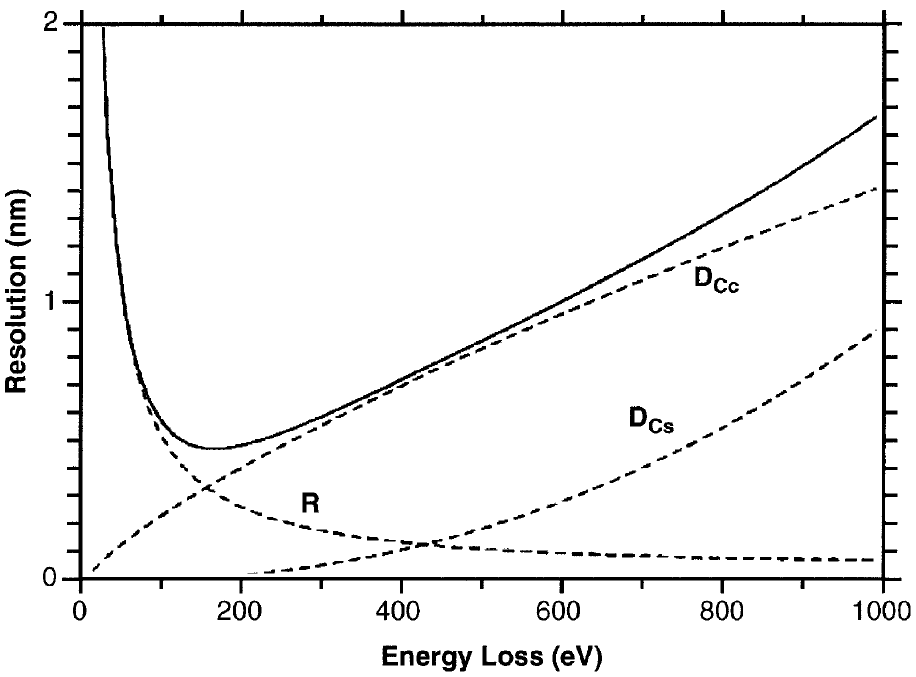
Figure 4971c. Theoretical plots of the spatial resolution of energy-filtered
images as a function of energy loss. [7]
Figure 4971d shows the dependence of the spatial resolution of the inelastic images on the accelerating voltage from 120 kV to 300 kV as a function of scattering angle (θ0). In this modeling [7], the energy loss was set to a constant at 500 eV in both cases (a) and (b). Figure 4971d indicates that the spatial resolution can be improved with increase of the accelerating voltage and Table 4971 shows the decrease of the energy slit width improves also the spatial resolution.
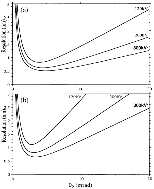
Figure 4971d. Schematic plots of the dependence of the spatial resolution of energy filtered images on the accelerating voltage. [7]
Table 4971. The best spatial resolution at 120 kV, 200 kV, and 300 kV (The numbers are extracted from Figure 4971d).
| |
Energy slit width |
10 eV |
20 eV |
| 120 kV |
0.9 nm |
1.12 nm |
| 200 kV |
0.7 nm |
0.82 nm |
| 300 kV |
0.5 nm |
0.68 nm |
Furthermore, the spatial resolution of EFTEM mapping can also be degraded by the specimen drifts during the slow acquisitions of the elemental images. Note that in the energy-loss-based imaging in most conventional TEMs, it is still very difficult to observe inelastic or elemental images at an atomic level resolution, because the spatial resolution for those techniques is in the range of 1 and 2 nm.
[1] Pennycook S. J., 1982. High resolution electron microscopy and
microanalysis. Contemp. Phys., 23, 371–400.
[2] Berger A., Kohl H., 1993. Optimum imaging parameters for elemental
mapping in an energy filtering transmission electron microscope.
Optik, 4, 175–193.
[3] Berger A., Kohl H., 1993. Elemental mapping using an imaging energyfilter:
image formation and resolution limits. Microsc. Microanal.
Microstr., 3, 159–174.
[4] Shuman H., Chang C. F., Somlyo A. P., 1986. Elemental imaging and
resolution in energy-filtered conventional electron microscopy.
Ultramicroscopy, 19, 121–134.
[5] Krivanek O. L., Kundmann M. K., Kimoto K., 1995. Spatial resolution in
EFTEM elemental maps. J. Microsc., 180, 277–287.
[6] Kurata H., Moriguchi S., Isoda S., Kobayashi T., 1996. Attainable
resolution of energy-selecting image using high-voltage electron
microscope. J. Electron Microsc., 45, 79–84.
[7] Yoshio Bando, Masanori Mitome, Dmitri Golberg, Yoshizo Kitami, Keiji Kurashima, Toshihiko Kaneyama, Yoshihiro Okura and Mikio Naruse, New 300 kV Energy-Filtering Field Emission Electron Microscope, Jpn. J. Appl. Phys. Vol. 40 (2001) pp. L1193 – L1196.
|