Technique |
Self C-contamination from tool |
Sensitivity for interface and low contents |
|
Artifacts |
Not good |
|
|
No |
Good |
FIB sample preparation |
Induces carbon contaminants |
|
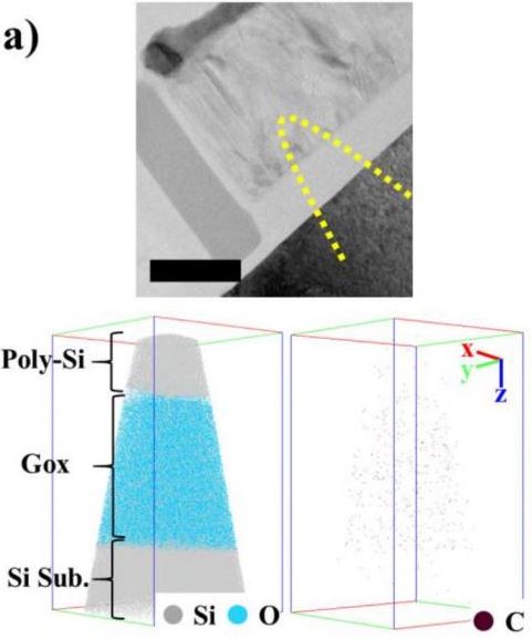
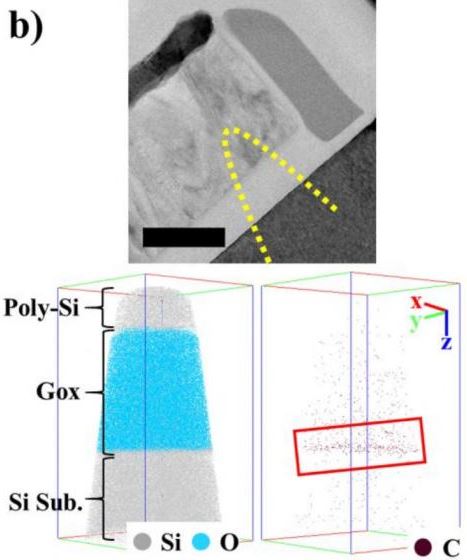
Figure 1211 shows cross-sectional TEM images and 3D APT maps of a good MOSFET structure and a failing MOSFET structure with a shifted threshold voltage, respectively. The 3D atomic images of a full section of the samples were obtained by ions collected from each sample. A small amount of carbon, piled up at the interface between the gate oxide (Gox) and Si substrate in the failing structure, was obviously detected by APT technique. However, such carbon content cannot be detected by using TEM-EDS technique due to its poor sensitivity or ToF-SIMS technique due to its poor spatial resolution.
| Figure 1211. Cross-sectional TEM images and 3D APT images: (a) Good MOSFET structure and (b) Failing MOSFET structure. The yellow dotted lines in the TEM images show the corresponding positions of the needle-shaped APT samples. The rectangular box in (b) indicates the detected carbon contents segregated at the interface of the gate oxide and Si substrate of the failing structure, while the good structure does not have such C segregation. [1] |
[1]
Ju-heon Kim, Euna Ok, Hyunmi Sim, Dongkeun Na, Ho Seok Song, Dae Hyun Kim, Yong-beom Cho, Seok-jun Won, Tae-Soo Park, Samsung Electronics Co., Ltd, Impact of carbon on threshold voltage shift in MOSFET studied by 3D atom probe tomography, Proceedings from the 43rd International Symposium for Testing and Failure Analysis, ISTFA 2017. |