Visibility of Electron Diffraction - Practical Electron Microscopy and Database - - An Online Book - |
||||||||
| Microanalysis | EM Book https://www.globalsino.com/EM/ | ||||||||
| ================================================================================= | ||||||||
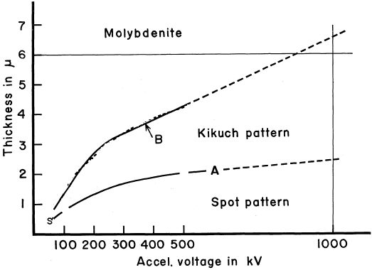
Figure 1232 shows the dependence of the appearance of electron diffraction and Kikuchi patterns on the TEM sample thickness and the accelerating voltages of the incident electron beam for molybdenite crystals. Diffraction patterns can be observed in the region below Curve A, while Kikuchi patterns can be observed between Curves A and B. Both diffraction and Kikuchi patterns can be simultaneously observed in the region slightly below and above Curve A. In general, the Curve B gives the maximum thickness for which dislocations can be observable.
[1] Uyeda, Ryozi; Nonoyama, Minoru, The Observation of Thick Specimens by High Voltage Electron Microscopy. Experiment with Molybdenite Films at 50-500 kV, Japanese Journal of Applied Physics, 6(5), pp. 557 (1967).
|
||||||||
| ================================================================================= | ||||||||
|
|
||||||||
