| In many cases, high energy resolution for EELS technique is needed to detect the point defects, grain boundaries and heterointerfaces in materials.
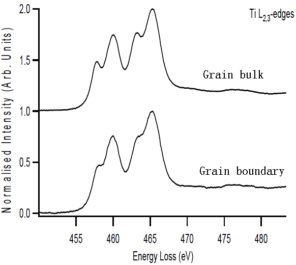
Figure 128a compares the EELS profiles taken from a grain boundary and a grain bulk of perovskite-type CaCu3Ti4O12 (with grain sizes of 100-300 µm). Based on HRTEM imaging, it was suggested that the grain boundary exhibited a step-like morphology and high local stress due to the change of chemistry and/or structure. The grain boundary was Cu rich, which was determined by EDS measurements.
| Figure 128a. Comparison of the EEL spectra of Ti L2,3-edges and Cu L2,3-edges between grain boundary and bulk of CaCu3Ti4O12. The valence states of Ti and Cu have been determined and listed in Table 128a. Adapted from [1] |
| Table 128a. Valence states of Ti and Cu in a grain boundary and a grain bulk of CaCu3Ti4O12. |
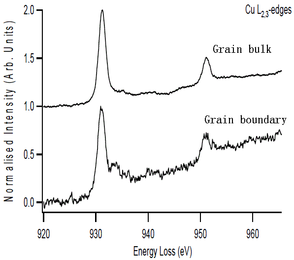
Figure 128b shows the Z-contrast image of a symmetric 24° [001] tilt grain boundary in YSZ (yttria-stabilized zirconia), the schematic of the grain boundary structure and the EEL spectra from the bulk and grain boundary after removal of EELS background. Table 128b lists the material properties which has been extracted from the EELS profiles. These properties may cause an increase of the number of electrons in the conduction band at the grain boundaries.
| Figure 128b. (a) Z-contrast image of a symmetric 24° [001] tilt grain boundary in YSZ (yttria-stabilized zirconia), (b) schematic of the grain boundary structure, and (c) EEL spectra from the bulk and grain boundary after removal of EELS background. [2] |
Table 128b. Material properties which has been extracted from the EELS profiles. |
| |
Property of grain boundary |
| M2,3 of Y |
1.5 eV shift to higher energy than bulk, indicating an increase in the number of electrons in the boundary plane |
| M2,3 of Zr |
| O K near-edge structure |
A change of O K near-edge structure indicates
the distortion of cubic symmetry at the grain boundary |
| M3/M2 ratios of Zr |
Larger than bulk, indicating an increase in the number of electrons in the boundary plane |
| M3/M2 ratios of Y |
| Y/Zr ratio |
Larger than bulk |
| O/Zr ratio |
Smaller than bulk |
| O/Y ratio |
Figure 128c shows an As-L2,3 EELS map and a line scan of As-doped Si BiCMOS n-p-n transistors with As detection sensitivity of 1019 cm–3 at a spatial resolution of ~2 nm, measured in a STEM system with an incident beam energy of 120 keV.
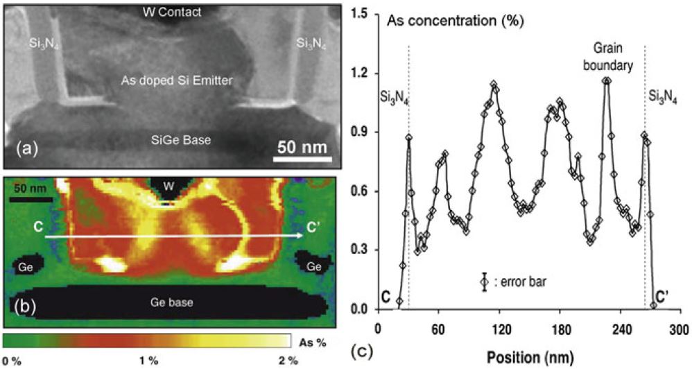
| Figure 128c. As-doped Si BiCMOS transistors: (a) STEM image, (b) As-L2,3 EELS map (150 × 60 pixels at 2 nm/pixel), and (c) Line scan along the white line in (b). As segregation at a grain boundary is observed. [3] |
[1] C.C. Calvert, W.M. Rainforth, D.C. Sinclair, and A.R. West, EELS analyses at grain boundaries in CaCu3Ti4O12, Journal of Physics Conference Series 02/2006; 26(1):65.
[2] Y. Ito, Y Lei, N.D. Browning and T.J. Mazanec, Analysis of the Atomic-Scale Defect Chemistry at Interfaces in Fluorite Structured Oxides by Electron Energy Loss Spectroscopy, Mat. Res. Soc. Symp. Proc. Vol. 703, 489 (2002).
[3] Servanton, G., and Pantel, R. (2010) Arsenic dopant mapping in state-of-the-art semiconductor
devices using electron energy-loss spectroscopy. Micron 41, 118–122.
|