TEM Lattice Fringe Affected by FIB Damage - Practical Electron Microscopy and Database - - An Online Book - |
||||||||
| Microanalysis | EM Book https://www.globalsino.com/EM/ | ||||||||
| ================================================================================= | ||||||||
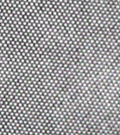
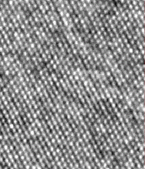
Figure 1310 shows HAADF lattice images of Si crystalline specimens prepared with 40 kV and 2 kV Ga+ Polishing. It is clear that the 40 kV milling caused more damage.
|
||||||||
| ================================================================================= | ||||||||
|
|
||||||||