Chapter/Index: Introduction | A | B | C | D | E | F | G | H | I | J | K | L | M | N | O | P | Q | R | S | T | U | V | W | X | Y | Z | Appendix
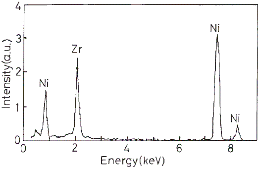
| Figure 1826a shows EDS profile of a Zr-Ni thin film. The Zr-L line is often chosen for quantification analysis.
Figure 1826a. EDS profile of a Zr-Ni thin film. [1] Figure 1826b shows a deconvoluted X-ray spectrum taken from a material containing Ta, Sr, Zr, Nb, and Pb elements. The different colored peaks represent the contribution of the various elements. The grey area is the background corrected spectrum which is the sum of all the deconvoluted lines.
[1] Masahiro Kitada and Fumiyoshi Kirino, Effects of Sputter Order and Oxide Layer on Amorphous Formation
of Zr-Ni Thin Film System, Materials Transactions, Vol. 46, No. 2 (2005) pp. 277 to 280.
|