|
This book (Practical Electron Microscopy and Database) is a reference for TEM and SEM students, operators, engineers, technicians, managers, and researchers.
|
=================================================================================
As shown in Figure 2013 (a), in contacts in Si ICs, a silicide is formed by depositing a metal onto Si, followed by heating the sample. The Al above the silicide can migrate through the silicide along the grain boundaries of the silicide, resulting in formation of Al/Si contacts as shown in Figure 2013 (b). This migration can be enhanced by the high compressive stress in the Al induced by its high CTE than that of Si (CTEAl>> CTESi) at high temperatures. Recently, barrier layers are introduced to address the migration problem as shown in Figure 2013 (c). These barrier layers have the properties of low contact resistance, and good chemical, electrical, and mechanical stabilities.
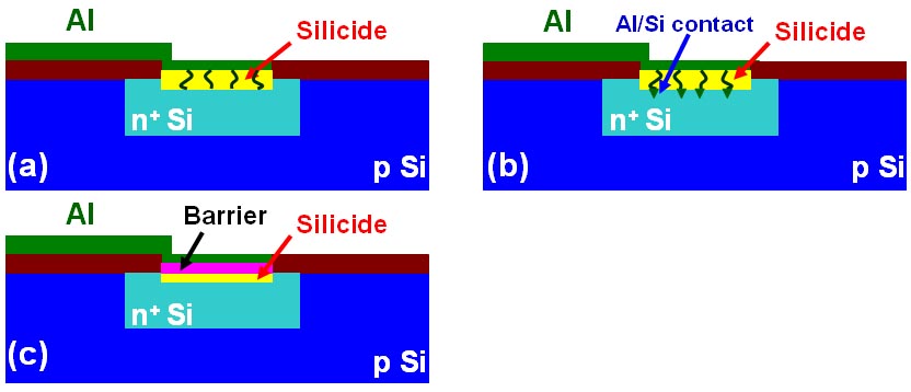
Figure 2013. (a) Silicides; (b) Formation of Al/Si contacts; and (c) Barrier layer between silicide and Si.
In IC (integrated circuits) applications, as a barrier layer it was confirmed that titanium nitride is superior to the Ti-W barrier metal and stoichiometric TiN exhibits low electrical resistivity (50-100 Ω-cm). Therefore, patterned TiN is a good material for microelectrode arrays [1].
Table 2013. Metallization selections in ICs.
Application |
Selection |
Gates, interconnection, and
contacts |
Polysilicon, refractory metal silicides (e.g. MoSix, TaSix, WSix, and TiSix), nitrides,aluminum, copper, and/or refractory metals. |
Diffusion barrier layer |
Ti, TiN, Ta, TaN, Ti-W alloy, and/or silicides |
Top level |
Aluminum, and/or copper |
Metallization
on silicon |
Silicides, tungsten, aluminum, and/or copper |
[1] L. A. Cyster, D. M. Grant, K. G. Parker, T. L. Parker, Biomol.Eng. 2002, 19, 171.
|