|
This book (Practical Electron Microscopy and Database) is a reference for TEM and SEM students, operators, engineers, technicians, managers, and researchers.
|
=================================================================================
Figure 2018 shows the historical view of Ohmic contact developments in Si(silicon)-based ICs. Ideally, Al (aluminum) would be deposited directly onto Si with perfect interfaces between Al and Si as shown in Figure 2018 (a). Unfortunately, the Si migrates into the Al, resulting in voids formed in the Si as shown in Figure 2018 (b). The Al can subsequently migrate into the formed voids, inducing spiking as shown in Figure 2018 (c). The big spike leads to junction shorts between n+ and p layers. Because the solubility of Si in Al is small (e.g. 0. 5 wt% at 450 °C), low Si doping in Al (1 to 3 wt% Si) suppresses spike formation significantly. However, other problems can occur subsequently, for instance, Al-doped p+ Si can precipitate out or p+ Si epitaxial layer can be formed between the original Si surface and the Al film as shown in Figure 2018 (d). Note that here Al is a p-type of dopants in Si. Furthermore, a challenge is that the formation probability of such epitaxial films is higher for (100)- than for (111)-oriented Si substrates. This can be more severe problem when the contact is scaled further and thus it only contains one or few grains.
Silicides were introduced to solve the precipitation problem. As shown in Figure 2018 (e), a silicide is formed by depositing a metal onto Si, followed by heating the sample. Here, the Al does not have to be doped with Si. However, the Al above the silicide can still migrate through the silicide along the grain boundaries of the silicide, resulting in formation of Al/Si contacts as shown in Figure 2018 (f). This migration can be enhanced by the high compressive stress in the Al induced by its high CTE than that of Si (CTEAl>> CTESi) at high temperatures. Recently, barrier layers are introduced to address the migration problem as shown in Figure 2018 (g). These barrier layers have the properties of low contact resistance, and good chemical, electrical, and mechanical stabilities.
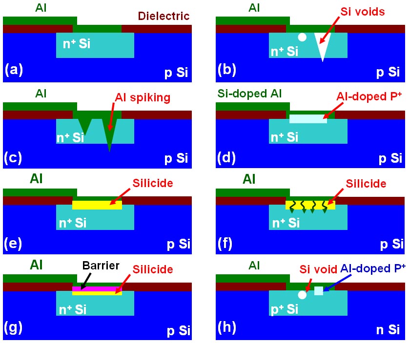
Figure 2018. Historical view of Ohmic contact developments in Si-based ICs: (a) Al deposited directly onto Si; (b) Voids formed in Si; (c) Al spiking; (d) p+ Si formation; (e) Silicides; (f) Formation of Al/Si contacts; and (g) Barrier layer/silicide.
|