Molybdenite (MoS2, molybdenum sulfide)
- Practical Electron Microscopy and Database -
- An Online Book -
| https://www.globalsino.com/EM/ |
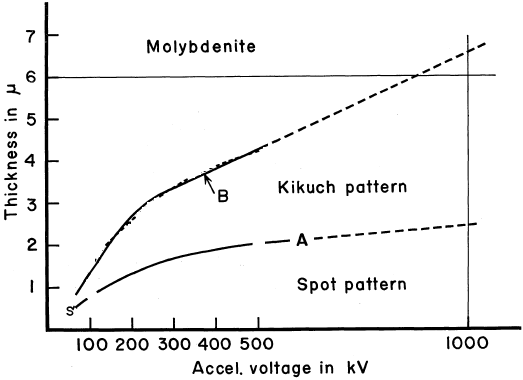
================================================================================= Molybdenum disulfide (MoS2) is a transition metal dichalcogenide and is formed by two-dimensional (2D) graphene-like S-Mo-S layers. The bonding within the layers is typically covalent and much stronger than the van der Waals forces between the layers, while the layers are held together by weak noncovalent interactions. In each layer, a Mo atom is covalently connected to six sulfur atoms, while each sulfur atom is bonded to three Mo atoms. On one hand, MoS2-based catalysts are attractive because they are active for both methanation and water-gas shift reactions, allowing for the reaction to occur at low H2/CO ratios. On the other hand, as a semiconducting compound, MoS2 is characterized by its layered crystal structure. It has been of interest because the behavior of electrons in the layers is quasi-two-dimensional. Plus, the interaction between layers can be modified by incorporating impurities between the layers in a process known as intercalation. Figure 2210a shows the dependence of the appearance of electron diffraction and Kikuchi patterns on the TEM sample thickness and the accelerating voltages of the incident electron beam for molybdenite crystals. Diffraction patterns can be observed in the region below Curve A, while Kikuchi patterns can be observed between Curves A and B. Both diffraction and Kikuchi patterns can be simultaneously observed in the region slightly below and above Curve A. In general, the Curve B gives the maximum thickness for which dislocations can be observable.
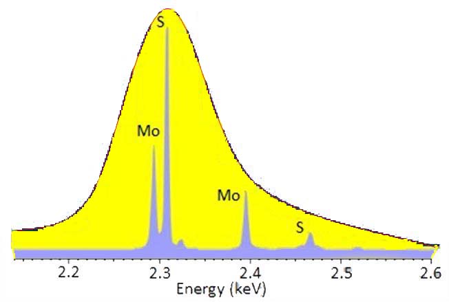
Figure 2210b shows the sulfur and molybdenum peaks overlap in the EDS spectrum, but are separated and sharp in the WDS spectrum.
Figure 2210b. Comparison of the EDS and WDS spectra taken from MoS2. Table 2210a. Properties of MoS2 compositions.
Table 2210b. Structural properties of some MoS2 compositions.
[1] Uyeda, Ryozi; Nonoyama, Minoru, The Observation of Thick Specimens by High Voltage Electron Microscopy. Experiment with Molybdenite Films at 50-500 kV, Japanese Journal of Applied Physics, 6(5), pp. 557 (1967).
=================================================================================
|