Chapter/Index: Introduction | A | B | C | D | E | F | G | H | I | J | K | L | M | N | O | P | Q | R | S | T | U | V | W | X | Y | Z | Appendix
| A dislocation can be observed in TEM because the lattice near the dislocation core is bent elastically. The degree of bending increases when closer to the dislocation core. Dark-field imaging mode, called weak-beam (WB) technique, is normally used for dislocation imaging. However, there are some factors which can affect the visibility (or called contrast) of dislocations and stacking faults. In TEM observation, dislocations become invisible if g•b = 0, i.e. b⊥g, and stacking faults with g•R=0 or g⊥R are invisible. Here,
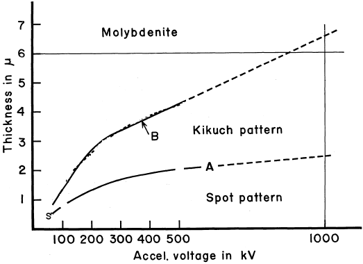
These conditions determine whether a dislocation or a stacking fault will be visible under TEM imaging. If these products are zero, the dislocation or fault becomes invisible due to the orientation of the vector relative to the dislocation or fault. Figure 2211 shows the dependence of the appearance of electron diffraction and Kikuchi patterns on the TEM sample thickness and the accelerating voltages of the incident electron beam for molybdenite crystals. Diffraction patterns can be observed in the region below Curve A, while Kikuchi patterns can be observed between Curves A and B. Both diffraction and Kikuchi patterns can be simultaneously observed in the region slightly below and above Curve A. In general, the Curve B gives the maximum thickness for which dislocations can be observable. No structures can be observed in the region above Curve B, while many structures can probably be observed in the region slightly below Curve B with a rather long exposure time.
[1] Uyeda, Ryozi; Nonoyama, Minoru, The Observation of Thick Specimens by High Voltage Electron Microscopy. Experiment with Molybdenite Films at 50-500 kV, Japanese Journal of Applied Physics, 6(5), pp. 557 (1967).
|