=================================================================================
In STEM mode, the radius of the Airy disc dd due to the diffraction limit is written as,
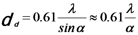 ------------------------------ [2238a] ------------------------------ [2238a]
where,
α -- The convergence semi-angle;
λ -- The wavelength of the incident electron beam.
Since the wavelength (λ) of the incident electrons increases at lower acceleration voltages, the convergence semi-angle (α) should be increased to achieve an Airy disc dd equivalent to that obtained at higher acceleration voltages.
On the other hand, the beam spreading caused by chromatic aberration dc can be given by,
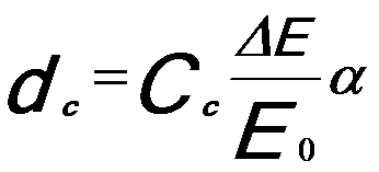 ---------------------------------- [2238b] ---------------------------------- [2238b]
where,
ΔE -- The energy spread of the electron beam;
E0 -- Eenergy of incident electron beam;
Cc -- The non-relativistic chromatic aberration and its coefficient.
From Equation 2238b we know that both Cc and ΔE should be low enough in order to suppress beam spreading at low acceleration voltages, especially since Cc depends strongly on the accelerating voltage.
In STEM-related measurements, it is possible to reduce the convergence of the electron beam and thus the tail produced by spherical aberration, by reducing the size of the C2 aperture, but this is at the expense of the total probe current.
Furthermore, the spatial resolution of STEM measurements is also determined by the specimen thickness, due to cone shape of the probe as shown in Figure 2238. For instance, if we have the experimental conditions below:
i) A specimen is in thickness of 600 nm.
ii) The incident electron spot size is ~1 nm.
iii) The convergence angle of the incident electron is 10 mrad.
Then, the diameter of the electron at the bottom surface of the specimen is about 10 nm. Therefore, the spatial resolution will be about 10 nm in diameter. Note that the specimen thickness is more critical when the semi-convergence angle is large, for instance, under Cs-corrected STEM condition.
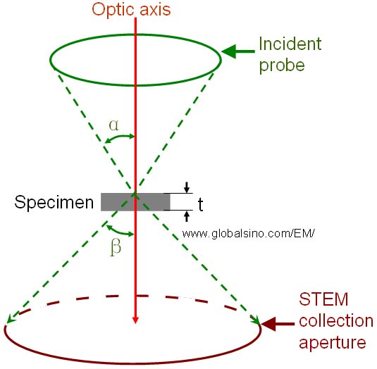
Figure 2238. Schematic illustration of incident and scattered electrons in STEM. α is the semi-convergence angle, while β is the semi-collection angle. t is the specimen thickness.
|