=================================================================================
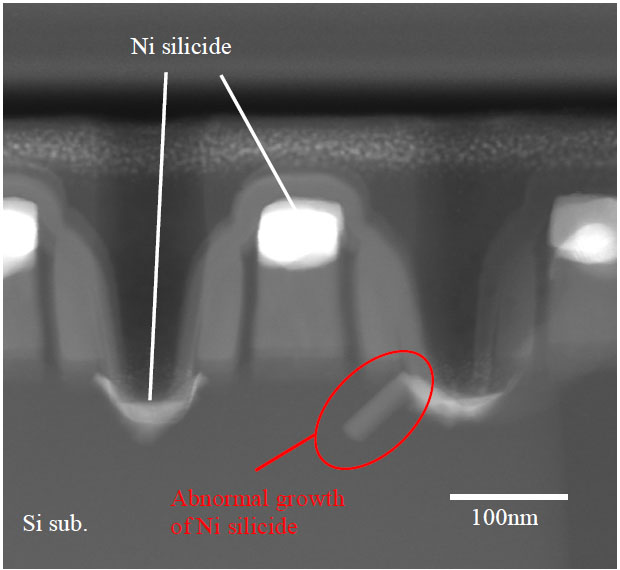
Kudo et al. [1] applied electron tomography to study abnormal growth of nickel silicide in silicon(Si)-based MOS structure in three-dimension (3-D). The cross-sectional STEM image of a MOS transistor in Figure 2445a presents nickel silicide penetration into junction due to the abnormal growth of the Ni silicide. This Ni silicide penetration induced junction leakage-current in the MOS transistor.

Figure 2445a. Nickel silicide penetration into junction of a MOS transistor due to the abnormal growth of the Ni silicide. [1]
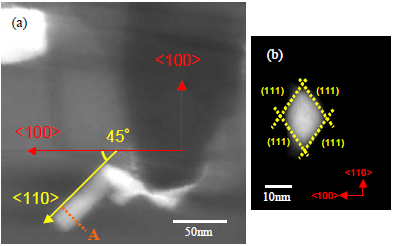
The tomographic image in Figure 2445b (a) determined that the abnormal growth (in Figure 2445a) occurred in <110> direction along a {111} plane, and Figure 2445b (b) shows a cross-sectional image that is perpendicular to the abnormal growth direction.

Figure 2445b. Images obtained by electron tomography technique: (a) A sliced image of the abnormal growth of Ni silicide in the Si-based MOS structure, and (b) The perpendicular cross-sectional image of the abnormal growth.
[1]
[1] S. Kudo, Y. Hirose, N. Hashikawa, T. Yamaguchi, K. Kashihara, K. Maekawa, K. Asai, N. Murata, K. Asayama and E. Murakami, Analysis of Ni Silicide Abnormal Growth Mechanism Using Advanced TEM Techniques, IEEE International Reliability Physics Symposium, 2008. IRPS (2008) 10074334.
|

