=================================================================================
The milling rate in FIB milling process is defined as the ratio of the volume of the milled material to the product of the beam current and irradiation time, given by,
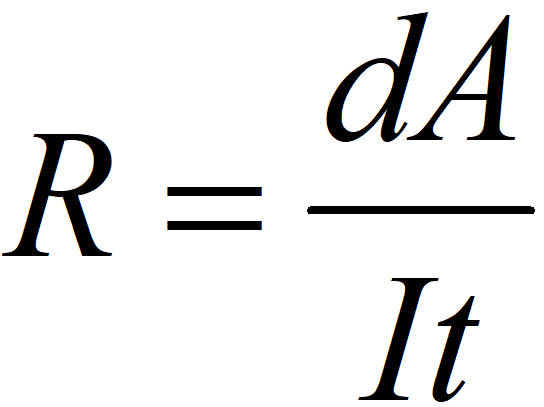 ---------------------------- [2454a] ---------------------------- [2454a]
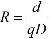 ---------------------------- [2454b] ---------------------------- [2454b]
where,
d - The milled depth,
A - The milled area,
I - The beam current,
t - The beam irradiation time,
q - The electronic charge,
D - The ion dose.
Therefore, the milling rate of materials depends on many factors, including the ion flux, the probability of sputtering per incident ion, the re-deposition of the sputtered material, and the angle of incidence of the ions with the sample surface. Table 2455 lists some examples of milling rates of different materials in FIB.
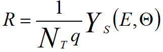
The correlation between the milling rate and the sputtering yield is given by,
 ---------------------------- [2454c] ---------------------------- [2454c]
where,
Nt - The atomic density of the target material,
YS(E,Θ) - The sputtering yield,
t - The beam irradiation time.
The user interfaces on the FIB systems normally have some configured files for sputtering of different materials. In these files, the beam dwell times and overlap have been calibrated for the specific materials in order to obtain the highest sputtering rates.
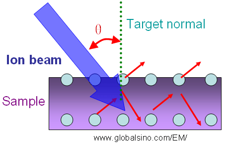
Figure 2454. The angle (θ) of incidence with respect to the target normal.
|