Chapter/Index: Introduction | A | B | C | D | E | F | G | H | I | J | K | L | M | N | O | P | Q | R | S | T | U | V | W | X | Y | Z | Appendix
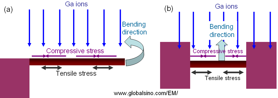
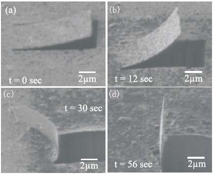
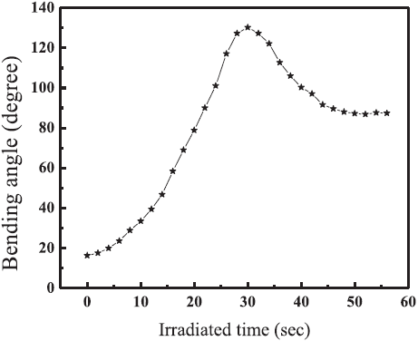
| Ion beam irradiation in FIB can induce stress redistribution, resulting in bending of cantilevers or TEM thin films. The stress redistribution can be induced by two reasons: Both the two mechanisms induce the stress difference between the top and bottom surfaces as shown in Figure 2486a. The top layer shrinks due to the generation of compressive stress, and then the atomic forces will affect the lower layers and a new equilibrium shape will be achieved with the film bending upwards. For instance, the SIM (scanning ion microscopy) images in Figure 2486b show the video-recorded process of Ag (silver) cantilever bending induced by ion irradiation in FIB. In this experiment, a focused 30-keV Ga ion beam with a flux of 2 × 10⁷ ions μm−2 s−1 was used to irradiate the cantilever at an angle of 52° (The standard configuration, see page2489) in a raster scan mode. The Ag cantilever had dimensions of 10 μm × 4 μm × 200 nm. The free end of the cantilever bent upwards, away from its original position (see Figure 2486b (a)). Figure 2486c shows the bending angle as a function of irradiation time. The bending rate is slow at the beginning, and then increases rapidly. The bending angle went beyond 90° and reached a maximum at ~130° (see Figure 2486b (c)). During further irradiation, the cantilever started bending backwards and finally the cantilever remained at 90°. This reverse bending occurred because of the further change of stress distribution due to ion irradiation on the bottom surface. On the other hand, the cantilever initially bent to form a curved structure; however, after it bent back across the 90° angle the curvature of the cantilever decreases, and finally it stayed almost a planar structure with a sharp bend of 90°. Furthermore, at low ion beam energies or with electron irradiation, no voids are created so that no bending occurred.
Figure 2486a. Schematic illustration showing the difference of ion-beam-induced stresses on the top and bottom surfaces of: (a) a cantilever, and (b) a TEM specimen prepared by FIB.
Figure 2486b. SIM snapshots showing the ion-beam-induced bending of an Ag nanocantilever at different irradiation times. Adapted from [3]
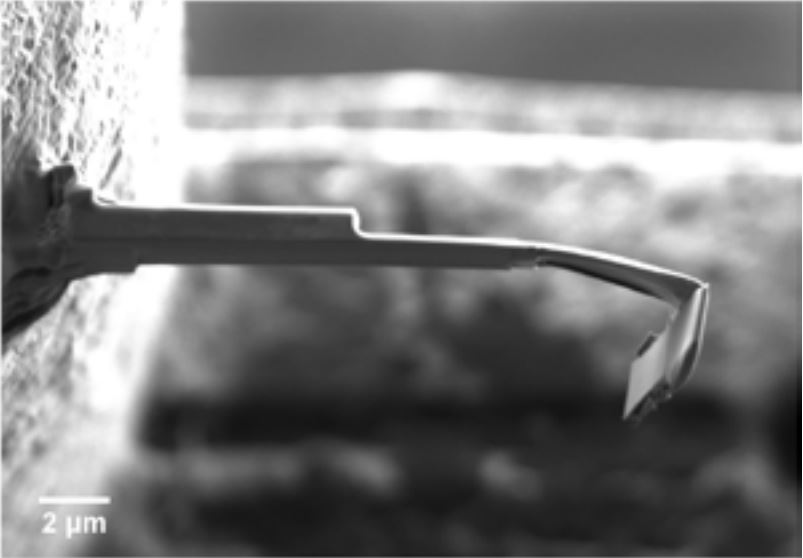
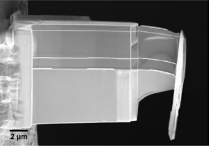
Figure 2486c. Bending angle of an Ag cantilever depending on the exposure time. [3] Note that because of the defect creation in FIB, imaging using SEM is recommended instead of SIM in dual beam SEM/FIB systems and the imaging time should be minimized in single beam FIB systems.Sample-mount method can result in different bending characteristics. For instance, as shown in Figure 2486d, side-mount polymer lamella develops very strong bending, so that further thinning is not possible. However, bottom-mount develops less bending.
[1] Medhekar N V, Chan W L, Shenoy V B and Chason E 2009
J. Phys.: Condens. Matter 21 224021.
|