|
|
Material Growth on Convex Surfaces
- Practical Electron Microscopy and Database -
- An Online Book -
|
|
https://www.globalsino.com/EM/
|
|
This book (Practical Electron Microscopy and Database) is a reference for TEM and SEM students, operators, engineers, technicians, managers, and researchers.
|
=================================================================================
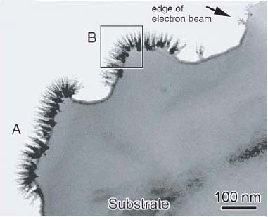
Charging effect in EBID (electron beam induced deposition) may enhance the formation of nano-dendrites, nano-whiskers, and nano-trees on insulator substrates (e.g. Al2O3 and SiO2). For instance, The TEM image in Figure 2509 shows the selectively formed tungsten (W) nano-dendrites on the convex surface of the substrate using hexacarbonyl (W(CO)6) precursor. It is necessary to highlight that the dendrites only formed on the convex surface even though the entire area of the image was irradiated by the incident electron beam. The gradient of the electric field induced by the accumulated charges on the convex surface of the substrate is normal to the surface so that the nano-dendrites grew parallel to the gradient of the electric field.

Figure 2509. Arrays of W nano-dendrites formed on the convex surface of an Al2O3 substrate by EBID with the electron beam intensity of 3.2 Acm−2 and the irradiation time of 30 s.
[1]
[1] Minghui Song and Kazuo Furuya, Fabrication and characterization of nanostructures on insulator substrates by electron-beam-induced deposition, Sci. Technol. Adv. Mater. 9 (2008) 023002.
|
=================================================================================
The book author (Yougui Liao) welcomes your comments, suggestions, and corrections, please click here for submission. If you let book author know once you have cited this book, the brief information of your publication will appear on the “Times Cited” page.
|
|
