|
|
Built-in Potential in p-n Junction
- Practical Electron Microscopy and Database -
- An Online Book -
|
|
https://www.globalsino.com/EM/
|
|
This book (Practical Electron Microscopy and Database) is a reference for TEM and SEM students, operators, engineers, technicians, managers, and researchers.
|
=================================================================================
The built-in potential Vbi in the p-n junction in semiconductors can be measured by off-axis electron holography, given by,
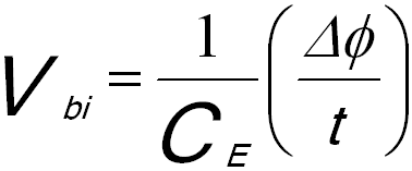 ------------------------------ [2552] ------------------------------ [2552]
where,
CE -- A constant dependent on the energy of the electron wave (e.g. 7.29 x 10⁻³ rad V−1 nm−1 for 200 kV electrons),
Δϕ -- The incident-electron phase change induced by the TEM specimen,
t -- The local thickness of the specimen.
For detailed discussion, see page4305.
|
=================================================================================
The book author (Yougui Liao) welcomes your comments, suggestions, and corrections, please click here for submission. If you let book author know once you have cited this book, the brief information of your publication will appear on the “Times Cited” page.
|
|