=================================================================================
The practical application of electron holography to various materials has been pioneered by some research groups, for instance, by one group at the Hitachi Advanced Research Laboratory in Japan [1]. Figure 2602a shows the most powerful TEM ever made, which is Hitachi 3 MeV.
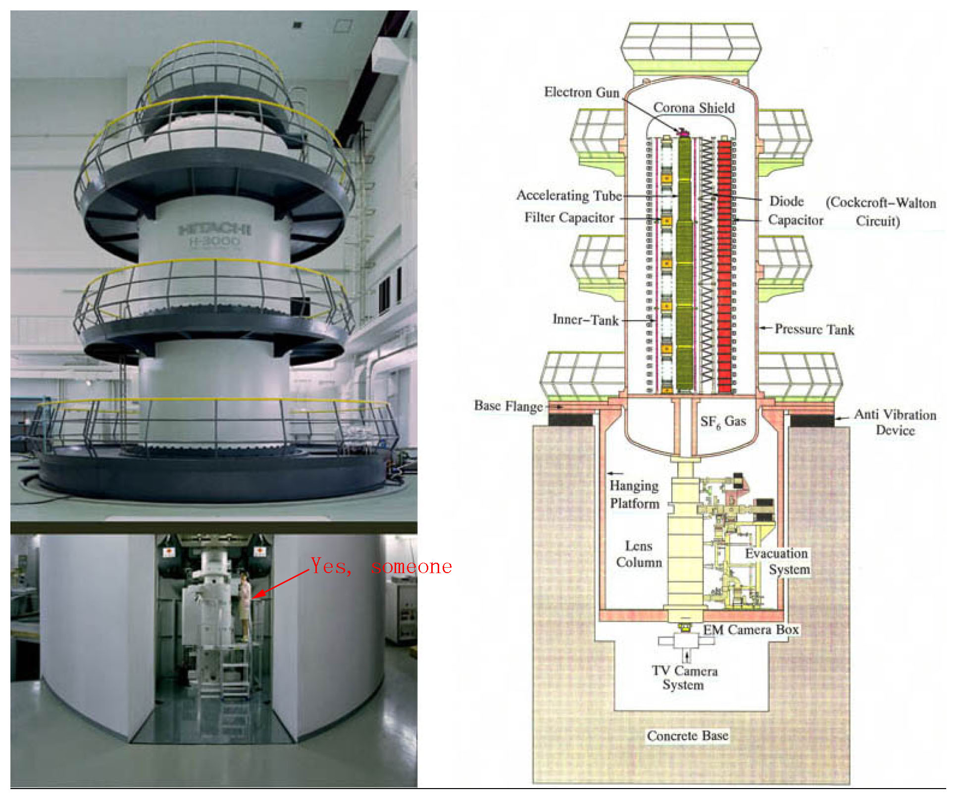
Figure 2602a. Hitachi 3 MeV: the most powerful TEM ever made.
Most modern scanning electron microscopes (SEMs) can record surface morphology but does not provide atomic resolution. The first atomic resolution, Hitachi aberration-corrected electron microscope, HD-2700C (page4444) was installed at Brookhaven National Laboratory [2].
[1] Tonomura, A. Electron Holography (Springer, 1999).
[2] Y. Zhu, H. Inada, K. Nakamura, and J. Wall, Imaging single atoms using secondary electrons with an aberration-corrected electron microscope, Nature Materials, 8 (2009) 808.
|