This enegy diagram described here is foundational in understanding the mechanisms behind electron emission processes and energy loss of incident electrons, which are critical in techniques such as X-ray photoelectron spectroscopy (XPS), Auger electron spectroscopy (AES) and EELS. These processes provide insights into the material's electronic structure, composition, and properties.
Figure 2634a shows the schematic illustration of the energy level diagrams for molecular structures with different number of atoms which are single atoms, dimers, clusters and bulk materials. Splitting of the atomic energy levels occurs when the single atoms form a diatomic molecule. As more atoms join the system, the levels split further until a quasi-continuous band structure is formed in the bulk material. In other words, quantum size effects occur when the quasi-continuous band structure of a solid state system begins to break down as more atoms are included.
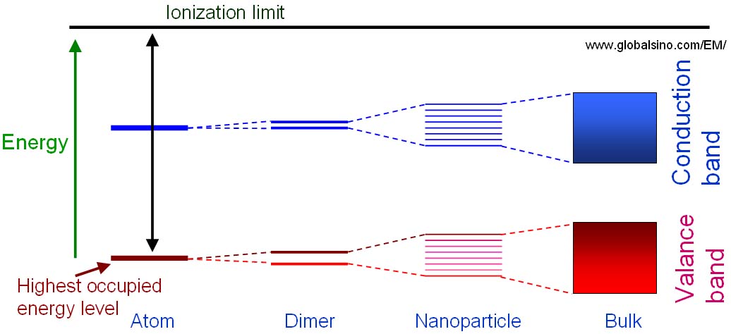
Figure 2634a. Schematic illustration of the energy level diagrams for molecular structures with different number of atoms which are single atoms, dimers, clusters and bulk materials. |
Figure 2634b shows an energy-level diagram of a solid with core-level excitation and electron emission processes at solid surface. This energy-level diagram provides a detailed view of the electronic structure of a solid, highlighting the core levels (K- and L-shells), the valence band, and critical energy levels such as the Fermi level (EF) and the vacuum level (Evac). The diagram illustrates the primary processes of electron excitation, where external energy sources, such as X-rays or incident electrons, can eject electrons from inner core levels (K and L). This excitation can lead to various secondary emission processes, including the emission of secondary electrons, photons (light and X-rays), and Auger electrons.
The Fermi level (EF) is shown as the energy level at which electrons are in equilibrium at absolute zero temperature, representing the dividing line between occupied and unoccupied electronic states. The vacuum level (Evac) indicates the energy threshold an electron must exceed to escape the solid into the vacuum. The valence band, represented as a shaded region, contains delocalized states where electrons are free to move throughout the material, playing a crucial role in its conductive properties.

Figure 2634b. Energy-level diagram of a solid with core-level excitation and electron emission processes at solid surface. |
In details, the diagram in Figure 2634b describes: - Energy Levels in a Solid:
- K- and L-shell Core Levels: The diagram illustrates the energy levels within an atom that are closest to the nucleus. These are known as core levels, with the K-shell being the innermost energy level (n=1) and the L-shell being the next level outward (n=2). These levels are deep within the energy well of the atom and are more tightly bound to the nucleus.
- Valence Band (Shaded Area): Above the core levels, there’s a shaded region representing the valence band. This band consists of delocalized states, meaning that the electrons are not bound to any particular atom but are free to move throughout the material. The valence band is crucial for the electrical properties of materials, as it is typically the highest range of electron energies that are still bound to atoms before the conduction band.
- Fermi Level (EF):
- The Fermi level
EF is represented as a horizontal line near the top of the shaded valence band. It signifies the energy level at which the probability of finding an electron is 50% at absolute zero temperature. In metals, the Fermi level lies within the valence band, allowing free electrons to contribute to electrical conduction.
- Vacuum Level (Evac):
- The vacuum level
Evac is the energy required for an electron to completely escape the material into the vacuum. This level is shown above all other levels, indicating that any electron reaching this energy can leave the solid.
- Primary processes (left side of the diagram):
- The diagram shows the primary processes of inner- and outer-shell excitation. This involves an external energy source, such as an X-ray photon or an incident electron, providing enough energy to eject an electron from an inner shell (K or L). This is depicted by arrows originating from the K and L levels, moving upward past the Fermi level towards the vacuum level.
- or example, if a photon strikes an electron in the K-shell with sufficient energy, it can excite that electron to a higher energy level, potentially allowing it to escape the material if it surpasses the vacuum level.
- Secondary processes (right side of the diagram):
- The right side of the diagram focuses on the secondary processes of photon and electron emission.
- Light (Photon Emission): When an electron from the valence band (or a higher shell) drops to fill a vacancy in a lower energy level (such as the L or K-shell), it can emit a photon. This is depicted by the wavy arrows labeled "Light" and "X-Ray" and represents the radiative transitions, where energy is released as electromagnetic radiation.
- Auger Electron Emission: This process occurs when the energy released from an electron dropping into a lower energy level is transferred to another electron, which is then emitted as an Auger electron. This is a non-radiative process, meaning no photon is emitted; instead, the energy directly ejects another electron.
- Secondary Electron Emission: Electrons that have absorbed enough energy (e.g., from an incident photon) but not enough to escape the solid can still be emitted from the material’s surface as secondary electrons. These are typically low-energy electrons that contribute to the secondary electron yield observed in techniques like scanning electron microscopy (SEM).
|