=================================================================================
Pearson et al. [1] experimentally and theoretically (based on one-electron Hartree-Slater calculations) found that the intensities of L2,3 white lines for most of the 3d and 4d transition metals decreased nearly linearly with increasing atomic number, reflecting the filling of the d states. Figure 3429a shows the deconvoluted and background-subtracted L2,3 energy-loss spectra for the 3d transition metals. The edge energies are not shown in order to present all the spectra in the same figure, while the intensities of the white lines are scaled simultaneously for all elements.
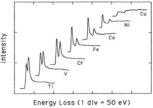
Figure 3429a. The deconvoluted and background-subtracted L2,3 energy-loss spectra for the 3d transition metals. [1]
Figure 3429b shows EEL spectra of TiO2, V, Cr, Fe2O3, CoO, NiO, and Cu with L2,3 energy-losses for the 3d transition metals. The chemical shift of O element in the different oxides (TiO2, Fe2O3, CoO, and NiO) is also indicated in the figure. The main edges of Ti, V, Cr, Fe, Co, Ni and Cu, and their edge onsets are listed in Table 3429a.
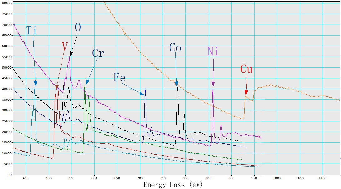
| Figure 3429b. EEL spectra of TiO2, V, Cr, Fe2O3, CoO, NiO, and Cu. |
Table 3429a. Main edges of Ti, V, Cr, Fe, Co, Ni, and Cu, and their edge onsets.
| Atomic number |
Element |
Edge(s) |
Edge onsets (eV) |
| 22 |
Ti |
L2,3 |
455 |
| 23 |
V |
L2,3 |
513 |
| 24 |
Cr |
L2,3 |
575 |
| 26 |
Fe |
L2,3 |
710 |
| 27 |
Co |
L2,3 |
779 |
| 28 |
Ni |
L2,3 |
855 |
| 29 |
Cu |
L2,3 |
935 |
The EEL spectra in Figure 3429c presents Co L2,3 edges in a series of Co–Rux–B-O catalysts (x = 0.7, 0.13, and 0). The intensities of Co L3 and L2 edge resonances are called white line, reflecting the occurrence of unoccupied states in the d band (2p → 3d transitions). The L3/L2 area ratio is sensitive to the oxidation state: The higher the L3/L2 area ratio, the more oxidized [4–6]. Here, L3/L2 area ratios are 1.4 for Rux = 0, 1.7 for Rux = 0.13, and 1.3 for Rux = 0.7.
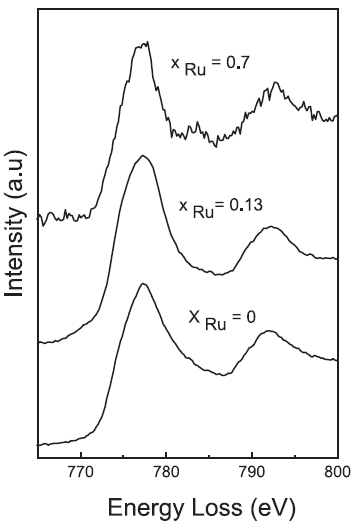
Figure 3429c. Co L2,3 edges in the EELS spectra of Co–Ru–B-O catalysts.
[3]
The valence state of Co can be indirectly determined by mapping the Si ELNES characteristics for the cases of CoSix (x = 1 or 2). Figure 3429d shows the as-measured and background-subtracted Si L2,3 EELS spectra of CoSi and CoSi2. The spectra for both silicides have Si L2,3 edge onsets located at 100.6 eV, while the Si ELNESs are slightly different. The CoSi2 ELNES has one broad peak with a characteristic pre-edge peak, while the CoSi ELNES does not show this pre-edge peak. Based on those characteristics, the parameters for three-window EFTEM method in Table 3429b are used. Here, in order to distinguish between CoSi and CoSi2, the pre-edge peak of CoSi2 was used, while the third peak of CoSi at 145 eV was used for the post-edge window. Using those settings, the Si ELNES maps of CoSi and CoSi2 were obtained together with TEM image as shown in Figure 3429e. Note that the Ti, Co, and Si elements have overlapped layers as indicated in Figure 3429e (a). Although the Ti film also gave some artefacts in the maps, it is very important that the grains consisting of CoSi and CoSi2 were still distinguished and the images revealed that a CoSi2 layer was formed between CoSi and Si substrate.
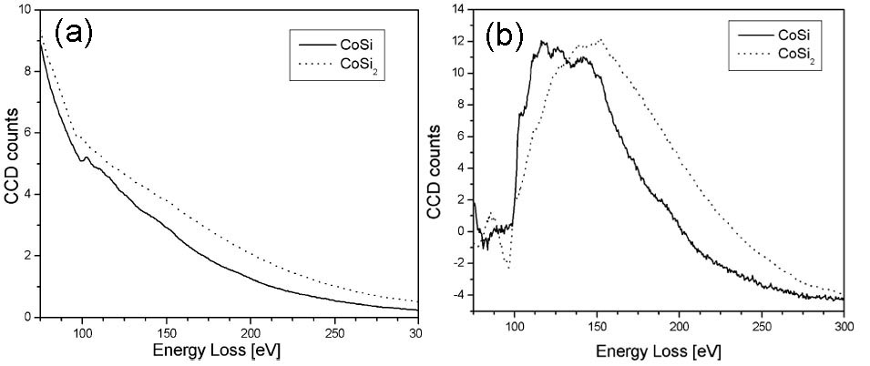
Figure 3429d. The as-measured (a), and background-subtracted (b) Si L2,3 EELS spectra of CoSi and CoSi2. Adapted from [2]
Table 3429b. Three-windows imaging filter settings for Si L2,3 ELNES for CoSi and CoSi2. [2]
| Compound |
Pre-edge window 1 (eV) |
Pre-edge window 2 (eV) |
Post-edge window (eV) |
Slit width (eV) |
CoSi |
125 |
130 |
145 |
10 |
CoSi2 |
67 |
77 |
91 |
6 |
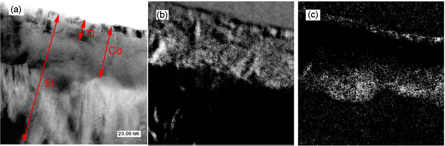
Figure 3429e. The TEM image (a), CoSi map (b), and CoSi2 map (c) of Ti/CoSi/CoSi2 layer stack. Adapted from [2].
[1] D. H. Pearson, C. C. Ahn, and B.Fultz, White lines and d-electron occupancies for the 3d and 4d transition metals, Physical Review B, 47(14), (1993) 8471-8478.
[2] M. Worch, H.J. Engelmann, W. Blum, E. Zschech, Cross-sectional thin film characterization of Si compounds in semiconductor device structures using both elemental and ELNES mapping by EFTEM, Thin Solid Films 405 (2002) 198–204.
[3] G.M. Arzac, T.C. Rojas, A. Fernández, New insights into the synergistic effect in bimetallic-boron catalysts for hydrogen generation: The Co–Ru–B system as a case study, Applied Catalysis B: Environmental 128 (2012) 39– 47.
[4] R.D. Leapman, L.A. Grunes, P.L. Fejes, Phys. Rev. B 26 (1982) 614.
[5] J.A. Horsley, J. Chem. Phys. 76 (1982) 1451.
[6] P.B. Oliate, T.C. Rojas, A. Fernández, A. Gedanken, Y. Koltypin, F. Palacio, Acta
Mater. 52 (2004) 2167–2171.
|