|
This book (Practical Electron Microscopy and Database) is a reference for TEM and SEM students, operators, engineers, technicians, managers, and researchers.
|
=================================================================================
Voyles et al [1] analyzed Sb (antimony) doped Si (silicon) in the <110> zone-axis orientation using ADF-STEM (annular dark-field scanning transmission electron microscopy) operated at 200 kV, directly observed individual Sb atoms at atomic-resolution, and identified the Sb clusters in Si responsible for the saturation of charge carriers. The size, structure, and distribution of these clusters were determined with a Sb-atom detection efficiency of almost 100%. The brightest dots on the left in the ADF-STEM image in Figure 3510 are atomic columns containing at least one Sb atom and the undoped region on the right shows no such very bright dots. Regarding the quality of the TEM sample, their simulations showed that for a Si column containing a single Sb atom to be more than 25% brighter than a pure Si column, the sample must be less than 50 Å thick. Random variations in thickness must be less than the contrast of one Sb atom, and the surfaces must be free from native amorphous SiO2 layers and amorphized bulk Si layers.
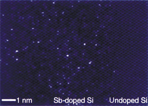
Figure 3510. ADF-STEM image of a cross section of highly Sb-doped Si.
[1] P. M. Voyles, D. A. Muller, J. L. Grazul, P. H. Citrin, and H.-J. L. Gossmann, Atomic-scale imaging of individual dopant atoms and clusters in highly n-type bulk Si, Nature, 416 (2002) 826.
|