=================================================================================
The achievable instrumental performance of a STEM is mainly determined by the size and shape of the incident electron probe. The most important optical factor in achieving the optimum probe profile is the radius of the probe-forming aperture, which determines the convergence semi-angle of the illumination. Small deviations from this optimum can degrade both the resolution and interpretability of the image contrast.
To form a fine, bright electron probe in the STEMs is important since the probe size limits the spatial resolution of imaging and analytical techniques such as electron energy-loss spectroscopy (EELS). The probe size and current in STEMs are mainly determined by the four factors (See page4954):
i) The effect of a finite source size (the ‘gun’), e.g. the source brightness,
ii) The geometric aberrations,
iii) The chromatic aberrations,
iv) The diffraction limit,
v) The instabilities.
In a simple geometric
optics approach these factors can be assumed to be
Gaussian. The overall probe size is the size of the demagnified electron source projected onto the specimen. This size also depends on the size of the virtual source that represents the electron gun and on the demagnification setting of the pre-specimen optical elements (mainly condenser lenses).
In STEM, the fluctuations in accelerating voltage or the current flow in the probe-forming electromagnetic lenses contributes to the chromatic aberration that leads a cutoff to the highest spatial frequency. In HRTEM, the cut-off frequency corresponds to the information limit. In STEM, the effect of the fluctuations induces additional contribution to the probe size [6],
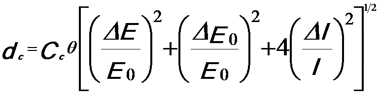 ------------- [3572] ------------- [3572]
where,
Cc -- The chromatic coefficient,
E0 -- The energy of the electron beam,
I -- The current in the probe-forming lens,
ΔE -- The spread in energy of the beam,
ΔE0 -- The fluctuation in the accelerating voltage,
ΔI -- The fluctuation of the lens current.
Figure 3572a shows the probe current as a function of focused probe (or spot) size in STEM mode and in microprobe mode in TEM.
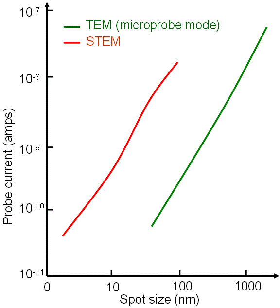
Figure 3572a. Probe current as a function of focused probe (or spot) size in STEM mode and in microprobe mode in TEM.
With small electron probes, e.g. ≤ 0.2 nm, STEM can obtain atomic resolution information from crystalline specimens and their defects [1 - 3]. For instance, in a Cs-corrected low-voltage STEM, Sasaki et al. [4] had the probe currents of ~7 pA and ~20 pA at 30 kV and at 60 kV, respectively. Using this system, they were able to obtain the atomic structure of Si (silicon) dumbbells of Si [110].
Figure 3572b shows the structure of the electron probe-forming system in STEM mode in JEOL JEM-2010F TEMs. A setup, consisting of electrostatic gun lens and twin condenser lens system, controls the de-magnification of the Schottky field emission source. Compared to the cold field emitter, the Schottky electron source has a much larger emission area. Each element of the electron source can be assumed to emit electrons incoherently and thus results in an incoherent broadening of the probe [5]. A large de-magnification factor between the source and probe reduces this probe-broadening effect. In addition, the beam current decreases due to the probe-forming aperture. A cross-over is formed between the two condenser lenses (C1 and C2) by employing near-maximum excitation in the C1 lens, resulting in a large source de-magnification. The C2 lens and the gun lens are used to tune the probe coherence further by setting the probe size. In the STEM mode, both condenser and objective mini-lenses are tuned off.
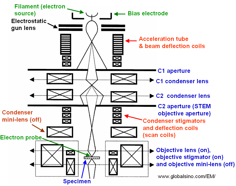
Figure 3572b. Schematic illustration of the probe-forming electron optics in STEM mode in JEOL JEM-2010F TEMs.
For the TEM configuration with a top-entry type EDS detector, the detector is placed above the objective lens in a TEM system with a high viewing angle (e.g. 70 °) to a horizontal specimen. Since the detector takes X-ray signals from the top of the objective lens, a large bore polepiece for the objective lens is needed. The use of such polepieces degrades the spatial resolution as well as the probe size.
In addition to the specimen itself, the X-ray generation process is also affected by the probe size, current, and convergence angle. Fortunately, elemental concentration quantification can be done with reasonable accuracy by comparing the peak intensities with k-factors in EDS spectra.
Most SEMs provide a final probe size less than 10 nm, but contain sufficient electron current to produce acceptable signal intensity from the specimen.
Table 3572. Examples of collection angles of EELS measurement in different microscope conditions.
| Accelerating voltage |
STEM |
Beam current |
Probe size |
Collection angle |
Aberration corrector |
reference |
| 200 keV |
CFEG |
7 pA |
0.12 nm |
31 mrad |
No corrector |
[7] |
| 100-200 pA |
|
15-25 mrad |
Cs-corrected |
[7] |
| 780 pA |
|
|
Cs/C5--corrected |
[7] |
[1] N.D. Browning, S.J. Pennycook, Direct experimental determination
of the atomic structure at internal interfaces, J.
Phys D 29 (1996) 1779 - 1798.
[2] N.D Browning, M.F. Chisholm, S.J. Pennycook, Atomic
resolution chemical analysis in the scanning transmission
electron microscope, Nature 366 (1993) 143 - 146.
[3] P.E. Batson, Simultaneous STEM and electron energy loss
spectroscopy with atomic column sensitivity, Nature 366
(1993) 727 - 729.
[4] Takeo Sasaki, Hidetaka Sawada, Fumio Hosokawa, Yuji Kohno, Takeshi Tomita, Toshikatsu Kaneyama, Yukihito Kondo, Koji Kimoto, Yuta Sato, and Kazu Suenaga, Performance of low-voltage STEM/TEM with delta corrector and cold field emission gun, Journal of Electron Microscopy 59(Supplement): S7–S13 (2010).
[5] J.M. Cowley, Image contrast in transmission scanning
electron microscopy, Appl. Phys. Lett. 15 (1969) 58-60.
[6] Spence JCH. High resolution electron microscopy. 3rd ed. Oxford: Clarendon Press; 2003.
[7] Peter W. Hawkes, Advances in Imaging and Electron Physics: Aberration-corrected Electron Microscopy, Volume 153, 2008.
|