Chapter/Index: Introduction | A | B | C | D | E | F | G | H | I | J | K | L | M | N | O | P | Q | R | S | T | U | V | W | X | Y | Z | Appendix
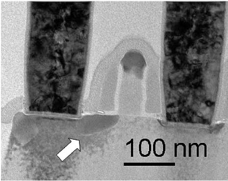
| The contrasts of SEM images can be basically categorized by topographic, material, and voltage contrast. The energy of Secondary Electrons (SE) is limited to a maximum value of 50 eV and is sensitive to local voltages around the emission point. Therefore, the local voltages at or around the beam-probed point give rise to a contrast which is called the voltage contrast. The voltage contrast method was discovered by Oatley and Everhart in 1957 [1] and has been mainly used in SEM application to IC measurement and e-beam testing. Voltage contrast: The voltage contrast can only be observed when there is a surface potential difference between the interesting structure and the adjacent structures. However, it should be mentioned that the surface potential exhibits dynamic characteristics so that the voltage contrast probably can only be detected at a certain period of electron irradiation. Figure 3843a shows a failure of S-RAM cell induced by uncontrolled diffusion of Ni under a spacer. Note that the failing S-RAM cell was first localized on a wafer by the voltage-contrast method using scanning electron microscopy (SEM).
Figure 3843b shows an example of VC defect detection from gate contact.
[1] Ura, K. and Fujioka, H. (1989) Electron beam testing. Adv. Electron.
Electron Phys., Vol. 73, pp. 233 - 317. Academic, New York.
|