|
|
PVC (Passive Voltage Contrast) of Transistors
- Practical Electron Microscopy and Database -
- An Online Book -
|
|
https://www.globalsino.com/EM/
|
|
This book (Practical Electron Microscopy and Database) is a reference for TEM and SEM students, operators, engineers, technicians, managers, and researchers.
|
=================================================================================
The passive voltage contrast (PVC) of MOS transistors can be complicated. For instance, the source contact should always give a dark signal if we just consider the pn junction behavior in PVC. However, as shown in Figure 3846 (b) it can give a bright signal because it is discharged through the grounded drain contact when the transistor is turned on due to the positive charges in the gate caused by the irradiation of the scanning incident ion beam through the silicon dioxide (SiO2) in FIB system. On the other hand, as shown in Figure 3846 (a) when this gate conductor is grounded the source contact appears dark. The gate grounding can be caused by FIB-welding or defective short between gate and drain.
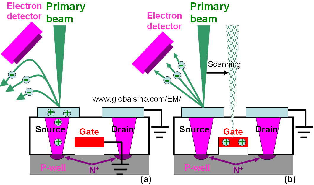
Figure 3846. Different cases of passive voltage contrast (PVC) of transistors.
|
=================================================================================
The book author (Dr. Liao) welcomes your comments, suggestions, and corrections, please click here for submission. You can click How to Cite This Book to cite this book. If you let Dr. Liao know once you have cited this book, the brief information of your publication will appear on the “Times Cited” page. This appearance can help advertise your publication.
|
|