|
|
Passive Voltage Contrast (PVC) of pn-Junction Structures/Diodes
- Practical Electron Microscopy and Database -
- An Online Book -
|
|
https://www.globalsino.com/EM/
|
|
This book (Practical Electron Microscopy and Database) is a reference for TEM and SEM students, operators, engineers, technicians, managers, and researchers.
|
=================================================================================
In integrated circuits (ICs), there are many contacts formed by combining doped materials, semiconducting materials, metals, and/or alloys. For instance, in Figure 3856 the contacts formed between the two doped regions results in pn junctions (diodes). The metal plug is positively charged in Figure 3856 (a) because the pn junction is reverse-biased due to the emission of secondary electrons (SEs), while it is not charged in Figure 3856 (b) because the pn junction is forward-biased. Therefore, the metal plug appears dark in Figure 3856 (a) while it appears bright in Figure 3856 (b).
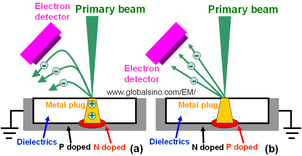
Figure 3856. Passive voltage contrast (PVC) of pn-junction structures.
|
=================================================================================
The book author (Dr. Liao) welcomes your comments, suggestions, and corrections, please click here for submission. You can click How to Cite This Book to cite this book. If you let Dr. Liao know once you have cited this book, the brief information of your publication will appear on the “Times Cited” page. This appearance can help advertise your publication.
|
|