|
|
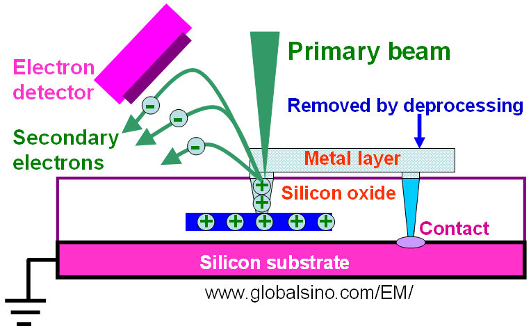
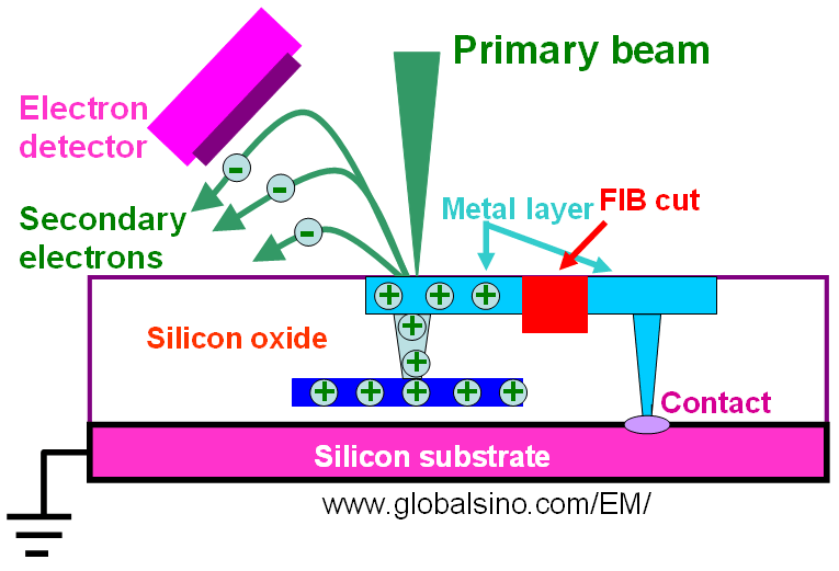
Artifacts in Passive Voltage Contrast (PVC) in FIB and SEM
The book author (Dr. Liao) welcomes your comments, suggestions, and corrections, please click here for submission. You can click How to Cite This Book to cite this book. If you let Dr. Liao know once you have cited this book, the brief information of your publication will appear on the “Times Cited” page. This appearance can help advertise your publication. |
|
||||||||||||
|
Copyright (C) 2006 GlobalSino, All Rights Reserved
|