=================================================================================
Ewald’s sphere was named after a German physicist and crystallographer, Paul Peter Ewald because of his relevant publications. He first applied this geometric construction in X-ray crystallography which illustrates the relationship between:
i) The wavelength of the incident and diffracted x-ray beams
ii) The diffraction angle of reflections (determined by Bragg condition)
iii) The reciprocal lattice of the crystal in the specimen
The purpose of the Ewald sphere is to determine which lattice planes will result in a reflection spot for the wavelength of an incident beam. The plane wave of the incident beam has a wave vector ki and the plane wave of the reflected beam has a wave vector kr. The difference between the wave-vectors of the reflected and incident waves can be given by scattering vector,
Δk = kr - ki ------------------------------ [3914a]
ki and kr have the same length, forming a sphere as shown in Figure 3914a. This sphere is called Ewald sphere.
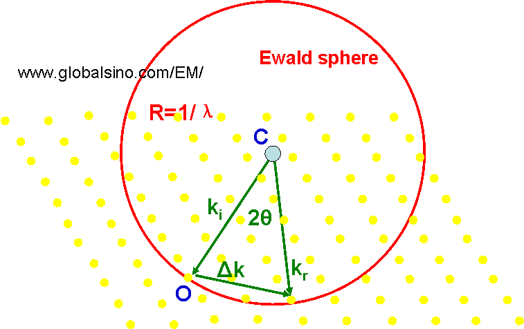
Figure 3914a. Schematic illustration of Ewald sphere construction.
The concept of Ewald’s sphere has later been used in electron and neutron crystallography. For TEM, because the crystal is a three-dimensional (3-D) structure, the reciprocal lattice is also a 3-D array of reflection points. The reflection signal shows up when the Ewald sphere intersects the reciprocal-lattice points (the Bragg condition is satisfied). Again, you should always imagine that the position of the reflected spot is in 3-D lattice, especially when you are studying crystallography of nanomaterials and small defects in crystals. In the case of TEM thin film, reflected relrods are formed. The spot position in the diffraction pattern moves because the Ewald sphere moves relative to the reciprocal lattice when the specimen or the electron beam is tilted.
Higher Order Laue Zones (HOLZs)
These outlying parts of a diffraction pattern are called Higher Order Laue Zones (HOLZs), which are defined by the interception of the Ewald sphere with the allowed HOLZ relrods in the reciprocal lattice. Each of the HOLZs can be described by the equation given by
hu + kv + lw = N -------------------------------- [3914b]
N -- An integer, called the order of the Laue zone.
[uvw] -- The direction of the incident electron beam.
hkl -- The coordinates of an allowed reflection in the Nth order Laue zone.
Therefore, HOLZ depends on the interplanar spacing in the crystal, the electron wavelength (i.e., the kV), L and any off-axis lens distortion. Ideal HOLZs are concentric at zero tilt, but increase their radius while moving off center to the upper left as the specimen is tilted. As examples, Figure 3914b shows FOLZ (First Order Laue Zones) and SOLZ (Second Order Laue Zones).
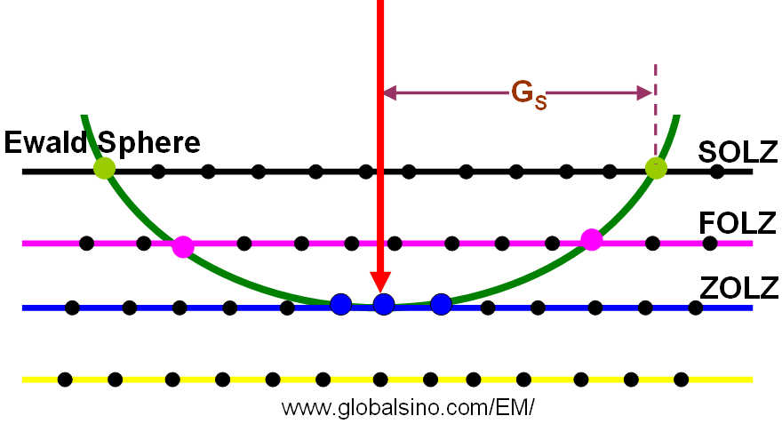
Figure 3914b. Schematic of ZOLZ, FOLZ, and SOLZ.
At higher angles the Laue condition is no longer satisfied so that the ZOLZ intensity decreases to zero. However, when the Ewald sphere intercepts the HOLZ planes of reciprocal lattice this diffraction intensity returns. Note that practically we rarely find higher order reflections because the Ewald sphere intercepts the HOLZ at large scattering angles.
The radius of the HOLZ rings is given by the interception of the Ewald sphere with the allowed HOLZ spots of the reciprocal lattice. In practice, the radius of the HOLZ ring is a direct measure of the interplanar spacing of the crystal along the direction of the directly transmitted electron beam and can be approximately given by,
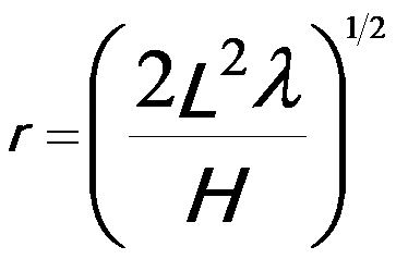 ----------------------------------- [3914] ----------------------------------- [3914]
where,
L -- The camera length,
λ -- The wavelength of the electron beam,
H -- The interplanar spacing of the crystal in the specimen.
The radius (r) of the Ewald sphere increases with decreasing electron wavelength λ; therefore, due to the small wavelength of electrons in TEM, the radius of the Ewald’s sphere is much larger than that of X-ray so that more reflected spots appear on the TEM screen or detector. In contrast to X-ray diffraction, the Ewald sphere is very flat for electron diffraction in TEM.
Note that distortion of diffraction spots in electron diffraction patterns can be caused by the curvature of the Ewald sphere.
|