Figure 3929. (a) Spot size and detection range of various techniques, and (b) Detection sensitivity versus spot size of probe. |
Table 3929a lists the resolution and sensitivity of
techniques for material characterizations. However, each of these values is obtained
under ideal conditions, and you will not have all of them optimized at the same time.
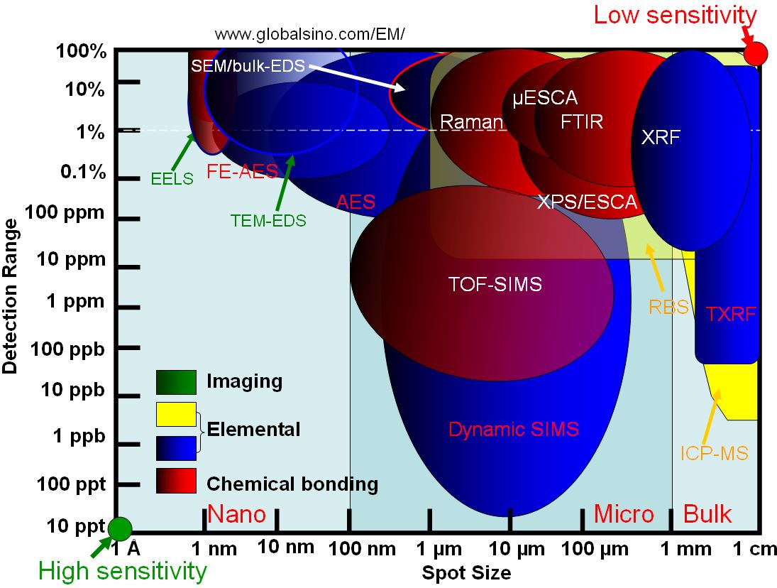
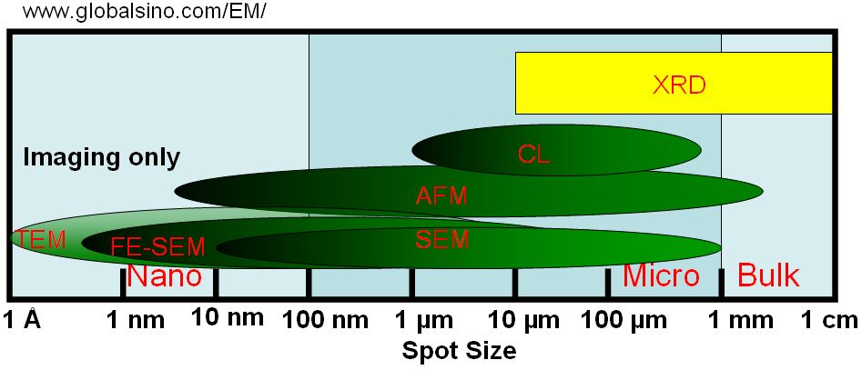
| Table 3929a. Resolution and sensitivity of
techniques for material characterizations. Spatial resolutions are < 5 nm in green, 5 ~ 50 nm in yellow, and > 50 nm in red.
Sensitivities are < 0.1% in green, 0.1% ~ 1% in yellow, and > 1% in red. |
| |
Probed depth |
Depth resolution |
Typical and best spatial resolution* |
Sensitivity to components |
|
|
0.2 nm |
0.5 nm (
Field of view: 150 nm) |
100 ppm |
Atomic Absorption Spectroscopy (AAA)
|
Outer atomic layers |
|
-- |
-- |
Auger electron spectroscopy (AES)
|
2 nm |
2-5 nm |
Typical: 20-100 nm; Best: < 2 nm; Common: 7 nm |
0.1% |
|
|
|
Best: 10, 000 nm |
|
|
10 nm-µm |
|
1 µm |
ppm |
|
|
< 1 µm |
|
~1 - 20 nm |
500 ppm (0.05%) - 1000 ppm 0.1% |
|
< 1 µm |
~1 µm |
~1 µm |
500 ppm (0.05%) - 1000 ppm 0.1% |
Electron energy-loss spectroscopy (EELS)
|
2-100 nm |
|
Typical: 1 nm; Best: < 1 nm |
1-Few % |
Electron Probe Microanalysis (EPMA)
|
1 µm |
|
0.5 µm |
100 ppm |
Elastic Recoil Spectrometry (ERS)
|
1 µm |
|
mm |
0.01% |
Extended X-Ray Absorption Fine Structure (EXAFS)
|
1 nm-Bulk
|
|
mm |
Few % |
Focused ion beam (FIB) |
|
|
5-100 nm |
|
Glow Discharge Mass Spectrometry (GDMS)
|
100 nm |
|
cm |
ppt-ppb |
Inductively Coupled Plasma Mass Spectrometry (ICP-MS)
|
5 µm |
|
mm |
ppt |
Inductively Coupled Plasma Optical Emission (ICP-Optical)/ICP optical emission spectrometry (ICP-OES)
|
5 µm |
|
mm |
ppb |
Infrared (Spectroscopy) (IR), e.g. Fourier Transform Infra-Red (Spectroscopy) (FTIR)
|
Few µm |
1 µm |
15-20 µm; Best: 3 µm |
Variable, Best 100 ppm |
Ion Scattering Spectrometry (ISS)
|
3 Å |
|
150 µm |
50ppm-l% |
Light
Microscopy |
Variable |
|
0.2 µm |
|
Low-Energy Electron Diffraction (LEED)
|
1 nm |
|
0.1 mm |
|
Local electrode atom probe (LEAP)
|
|
|
Best: < 0.1 nm |
|
Laser lonization Mass Spectrometry (LIMS)
|
100 nm |
|
2 µm |
l-100 ppm |
Laser Microprobe Mass Analysis (LAMMA)
|
|
|
Best: 1, 000 nm |
|
Medium-Energy Ion Scattering (MEIS)
|
1 nm |
|
mm |
0.1-10% |
Magneto-Optic Kerr Rotation (MOKE)
|
30 nm |
|
0.5 µm |
-- |
|
1 µm |
|
100 µm |
ppm |
Photoelectron microscopy (PEM or PEEM)
|
|
|
Best: < 0.5 nm |
|
Neutron Activation Analysis (NAA)
|
Bulk |
|
|
ppt-ppm |
|
Bulk |
|
|
|
|
Up to mm |
|
|
-- |
Nuclear Reaction Analysis (NRA)
|
10-100 nm |
|
10 µm |
10-100 ppm |
Particle Induced X-Ray Emission (PIXE)
|
Few µm |
|
100 µm |
10 ppm |
Proton-induced x-ray emission (PIXE)
|
|
|
Best: < 500 nm |
|
|
|
Few µm |
|
Few µm |
ppb |
Raman Spectroscopy (Raman)
|
Few µm |
|
1 µm |
Variable |
Rutherford backscattering spectroscopy (RBS)
|
2 µm |
10 nm |
mm; Best: ~ 1 µm |
0.01% (100 ppm) - 10% |
Reflected High Energy Electron Diffraction (RHEED)
|
1 nm |
|
0.01-0.02 mm |
|
Surface Analysis by Laser lonization (SALI)
|
3 Å |
|
100 nm |
ppb-ppm |
Scanning Electron Microscopy/Scanning Electron Microprobe/Secondary Electron Miscroscopy (SEM)
|
sub µm |
|
Typical: 2- 10 nm |
|
Scanning Force Microscopy (SFM)
|
sub Å |
|
1 nm |
|
Dynamic Secondary Ion Mass Spectrometry (Dynamic SIMS)
|
2 nm |
10 nm |
1 µm; Best: 200 nm |
ppb-ppm. E.g., B: 0.002-0.01 ppm; Be, Cr and Mn: 0.002 ppm; P: 0.1 ppm; Cu, Zn, As and Al: 0.2 ppm; Si, Sn and Ge: 0.5 ppm; S, Sb and C: 1.0 ppm; O and N: 10 ppm; H: 100 ppm
|
Nano-SIMS |
|
1 nm |
50 nm (Field of view:10 µm) |
9 ppm |
Static Secondary Ion Mass Spectrometry (Static SIMS)
|
3 Å |
|
100 µm |
Few % |
Sputtered Neutrals Mass Spectrometry/Secondary Neutrals Mass Spectrometry (SNMS)
|
~2 nm |
|
cm |
50 ppm |
Spark Source Mass Spectrometry (SSMS/Spark Source)
|
3 µm |
|
cm |
0.05 ppm |
Scanning Tunneling Microscopy (STM)
|
sub Å |
|
1 Å |
|
Conventional Transmission Electron Microscopy (CTEM)
|
1 - 200 nm |
|
1 nm - 5 nm |
|
Bright field (BF)- Scanning Transmission Electron Microscopy (STEM) and HAADF
|
100-200 nm |
|
Best: < 0.1 nm |
|
Selected Area Diffraction (SAD) in TEM
|
|
|
Best: 10 - 1000 nm |
|
Convergent Beam Electron Diffraction (CBED) in TEM
|
|
|
Best: 10 - 1000 nm |
> 0.1% changes in lattice parameter arising from compositional gradients |
Ultraviolet photoelectron spectroscopy (UPS)
|
1 nm |
|
Typical: mm; Best: < 1 µm |
|
Variable Angle Spectroscopic Ellipsometry (VASE)
|
1 µm |
|
cm |
-- |
Wavelength Dispersive (X-Ray) Spectroscopy (WDS/WDX)
|
|
|
|
0.01 - 0.1% |
X-ray photoelectron spectroscopy (XPS)
|
3 nm |
2 nm |
Typical: 100–150 µm; Best: 1 µm |
0.1 - 1% |
X-Ray Photoelectron Diffraction (XPD)
|
3 nm |
|
150 µm |
1% |
|
10 µm |
|
Typical: mm; Best: < 25 nm |
3% |
X-Ray Fluorescence Spectroscopy (XFS)
|
10 µm |
|
mm |
0.1% |
Total Reflection X-Ray Fluorescence (TXRF)
|
3 nm |
1 nm |
1 mm - cm |
ppb-ppm |
X-ray absorption spectroscopy (XAS)
|
|
|
Best: < 20 nm |
|
X-ray emission spectroscopy (XES)
|
|
|
Best: 1.5 – 10 nm |
|
| * The best spatial resolution is the spatial resolution limit which can be reached by the modern instruments, but it is probably not the resolution limit of your instrument. |
Table 3929b. Matrix of microanalysis techniques for material characterizations.
| Probe |
Signal |
| Electron |
Ion |
Photon |
| Electron |
Auger electron spectroscopy (AES)
✔ Scanning Auger Microscopy (SAM)
✔ Scanning Auger Microprobe (SAM)
✔ Auger Electron Diffraction (AED)
✔ Angular Distribution Auger Microscopy (ADAM)
✔ Kinetic Energy (KE)
✔ Cylindrical Mirror Analyzer (CMA)
Electron Energy Loss Spectroscopy (EELS)
✔ Reflection Electron Energy-Loss Microscopy (REELM)
✔ Reflected Electron Energy-Loss Spectroscopy (REELS)
✔ Extended Energy-Loss Fine Structure (EXELFS)
✔ Electron Energy-Loss Fine Structure (EELFS)
✔ Valence Electron Energy-Loss Spectroscopy (VEELS)
Scanning Electron Microscopy (SEM)
✔ Secondary Electron (SE)
✔ Backscattered Electron (BSE)
✔ Secondary Electron Microscopy with Polarization Analysis (SEMPA)
Transmission Electron Microscopy (TEM)
✔ Conventional Transmission Electron Microscopy (CTEM)
✔ Bright field (BF)- Scanning Transmission Electron Microscopy (STEM)
✔ High-angle annular dark- field (HAADF)
✔ High Resolution Transmission Electron Microscopy (HRTEM)
✔ Selected Area Diffraction (SAD)
✔ Analytical Electron Microscopy (AEM)
✔ Convergent Beam Electron Diffraction (CBED)
✔ Lorentz Transmission Electron Microscopy (LTEM) |
|
Cathodoluminescence (CL)
Energy Dispersive X-Ray Spectroscopy (EDS or EDX)
Wavelength Dispersive (X-Ray) Spectroscopy (WDS/WDX)
X-ray emission spectroscopy (XES)
Electron probe microanalysis (EPMA) |
| Ion |
|
Local electrode atom probe (LEAP)
Rutherford backscattering spectroscopy (RBS)
Secondary Ion Mass Spectrometry (SIMS)
✔ Dynamic Secondary Ion Mass Spectrometry (Dynamic SIMS)
✔ Static Secondary Ion Mass Spectrometry (Static SIMS)
✔ SIMS using a Quadruple Mass Spectrometer (Q-SIMS)
✔ SIMS using a Magnetic Sector Mass Spectrometer (Magnetic SIMS)
✔ Sector SIMS (Magnetic SIMS)
✔ SIMS using Time-of-Flight Mass Spectrometer (TOF-SIMS)
✔ Post lonization SIMS (PISIMS)
Ion Scattering Spectroscopy (ISS) |
Proton-induced x-ray emission (PIXE) |
| Photon |
Photoelectron microscopy (PEM or PEEM)
Ultraviolet photoelectron spectroscopy (UPS)
X-ray photoelectron spectroscopy (XPS) |
Laser Microprobe Mass Analysis (LAMMA) |
Bare human eyes
X-RayDiffraction (XRD)
✔ Grazing Incidence X-Ray Diffraction (GIXD/GIXRD)
✔ Double Crystal Diffractometer (DCD)
X-Ray Fluorescence spectroscopy (XRF)
✔ X-Ray Fluorescence Spectroscopy (XFS)
✔ Total Reflection X-Ray Fluorescence (TXRF)
✔ Total Reflection X-Ray Fluorescence (TRXFR)
X-ray absorption spectroscopy (XAS)
Total Reflection X-Ray Fluorescence (TXRF)
Fourier Transform Infra-Red (Spectroscopy) (FTIR) |
|
The glossary in Table 3929c lists alphabetically all the techniques used for material characterizations and the subsets of the techniques. The terminology of the techniques are also listed.
Table 3929c. Techniques for material characterizations and their typical capabilities.
| |
Analyses |
Vacuum |
Instrument cost per tool |
Usage |
|
Elemental
|
Chemical state |
Phase
|
Defect |
Surface |
Imaging |
Lattice |
Others |
Atomic Absorption Spectroscopy (AAA)
|
|
|
|
|
|
|
|
Yes |
Need |
|
Medium |
Large surface area |
|
Vapor Phase Decomposition-Atomic Absorption Spectroscopy (VPD-AAS)
|
|
|
|
|
|
|
|
|
|
|
|
|
Graphite Furnace Atomic Absorption (GFAA)
|
|
|
|
|
|
|
|
|
|
|
|
|
Flame Atomic Absorption (FAA)
|
|
|
|
|
|
|
|
|
|
|
|
|
Auger electron spectroscopy (AES)
|
Scanning Auger Microscopy (SAM)
|
Yes |
Yes |
|
|
|
Yes |
|
|
Need |
>$330k |
Extensive |
All solid, but usually inorganic materials
|
Scanning Auger Microprobe (SAM)
|
Auger Electron Diffraction (AED)
|
Angular Distribution Auger Microscopy (ADAM)
|
|
Cylindrical Mirror Analyzer (CMA)
|
Atom Inelastic Scattering (AIS)
|
|
|
|
|
|
|
|
|
|
|
|
|
|
|
|
|
|
|
|
|
|
|
|
|
|
Brunauer, Emmett, and Teller equation (BET)
|
|
|
|
|
|
|
|
|
|
|
|
|
Bidirectional Scattering Distribution Function (BSDF)
|
Bidirectional Reflective Distribution Function (BRDF)
|
|
|
|
|
|
|
|
|
|
|
|
|
Bidirectional Transmission Distribution Function (BTDF)
|
|
|
|
|
|
|
|
|
|
|
|
|
|
|
Yes |
|
Yes |
|
|
|
Yes |
Need |
<$60k |
Not common |
All solids, usually semiconductors |
Confocal Scanning Laser Microscope (CLSM)
|
|
|
|
|
|
|
|
|
|
|
|
|
Energy Dispersive (X-Ray) Spectroscopy (EDS)/Energy Dispersive X-Ray Spectroscopy (EDX)
|
|
Yes |
|
|
|
|
Yes |
|
|
Need |
$150 - 400k |
Medium |
All solids with Z> 5 |
|
|
|
|
|
|
|
Extensive |
Electron Energy Loss Spectroscopy (EELS)
|
High-Resolution Electron Energy-Loss Spectroscopy (HREELS)
|
|
Yes |
|
|
Yes |
|
|
|
Need |
>$330k |
Not common |
All solids |
Reflected Electron Energy-Loss Spectroscopy (REELS)
|
Yes |
Yes |
|
|
|
Yes |
|
|
Need |
|
Not common |
All solids |
Reflection Electron Energy-Loss Microscopy (REELM)
|
|
|
|
|
|
|
|
|
|
|
|
|
Low-Energy Electron-Loss Spectroscopy (LEELS)
|
|
|
|
|
|
|
|
|
|
|
|
|
Parallel (Detection) Electron Energy-Loss Spectrscopy (PEELS)
|
|
|
|
|
|
|
|
|
|
|
|
|
Extended Energy-Loss Fine Structure (EXELFS)
|
|
|
|
|
|
|
|
|
|
|
|
|
Electron Energy-Loss Fine Structure (EELFS)
|
|
|
|
|
|
|
|
|
|
|
|
|
Core Electron Energy-Loss Spectroscopy (CEELS)
|
|
|
|
|
|
|
|
|
|
|
|
|
Valence Electron Energy-Loss Spectroscopy (VEELS)
|
|
|
|
|
|
|
|
|
|
|
|
|
|
Electron energy-loss spectroscopy (EELS)
|
Yes |
Yes |
|
|
|
Yes |
|
|
Need |
>$500k |
Medium |
All solid thin films |
Electron Probe Microanalysis (EPMA)
|
Yes |
|
|
|
|
Yes |
|
|
Need |
>$330k |
Medium |
All solids |
Elastic Recoil Spectrometry (ERS)
|
|
|
|
|
|
|
|
Yes |
Need |
|
Not common |
Contain H |
Hydrogen Forward Scattering (HFS)
|
|
|
|
|
|
|
|
|
|
|
|
|
Hydrogen Recoil Spectrometry (HRS)
|
|
|
|
|
|
|
|
|
|
|
|
|
Forward Recoil Spectrometry (FRS)
|
|
|
|
|
|
|
|
|
|
|
|
|
Elastic Recoil Detection Analysis (ERDA)
|
|
|
|
|
|
|
|
|
|
|
|
|
Elastic Recoil Detection (ERD)
|
|
|
|
|
|
|
|
|
|
|
|
|
Particle Recoil Detection (PRD)
|
|
|
|
|
|
|
|
|
|
|
|
|
Extended X-Ray Absorption Fine Structure (EXAFS)
|
Surface Extended X-Ray Absorption Fine Structure (SEXAFS)
|
Yes |
|
|
|
Yes |
|
|
|
Need |
|
Not common |
Surface & adsorbate |
Near-Edge X-Ray Absorption Fine Structure (NEXAFS)
|
Yes |
|
|
|
|
|
|
X-Ray Absorption Near-Edge Structure (XANES)
|
|
|
|
|
|
|
Need or no need |
|
All solids |
X-Ray Absorption Fine Structure (XAFS)
|
|
|
|
|
|
|
|
Ferromagnetic Resonance (FMR)
|
|
|
|
|
|
|
|
|
|
|
|
|
|
Orientation ordering, local geometric packing of atoms |
|
|
|
|
Focused ion beam (FIB) |
|
|
|
|
|
Yes |
|
|
Need |
> $ 1M |
Extensive |
All solids |
Glow Discharge Mass Spectrometry (GDMS)
|
Glow Discharge Mass Spectrometry using a
Quadruple Mass Analyser (GDQMS)
|
Yes |
|
|
|
|
|
|
|
Need |
>$330k |
Medium |
Sample forms electrode |
Inductively Coupled Plasma Mass Spectrometry (ICP-MS)
|
Inductively Coupled Plasma (ICP)
|
Yes |
|
|
|
|
|
|
|
Need |
$60-330k |
Extensive |
All solids |
Laser Ablation ICP-MS (LA-ICP-MS)
|
|
|
|
|
|
|
|
Inductively Coupled Plasma Optical Emission (ICP-Optical)/ICP optical emission spectrometry (ICP-OES)
|
Inductively Coupled Plasma (ICP)
|
Yes |
|
|
|
|
|
|
|
Need |
<$60k |
Extensive |
All solids |
Inelastic Electron Tunneling Spectroscopy (IETS)
|
|
|
|
|
|
|
|
|
|
|
|
|
Infrared (Spectroscopy) (IR)
|
Fourier Transform Infra-Red (Spectroscopy) (FTIR)
|
|
Yes |
|
Yes |
|
|
|
Yes |
No need |
$60-330k |
Extensive |
All solids |
Gas Chromatography FTIR (GC-FTIR)
|
|
|
|
|
|
|
|
|
|
|
|
|
|
|
|
|
|
|
|
|
|
|
|
|
|
Attenuated Total Reflection (ATR)
|
|
|
|
|
|
|
|
|
|
|
|
|
Reflection Absorption (Spectroscopy) (RA)
|
|
|
|
|
|
|
|
|
|
|
|
|
Infrared Reflection Absorption Spectroscopy (IRAS)
|
|
|
|
|
|
|
|
|
|
|
|
|
Ion Scattering Spectrometry (ISS)
|
Yes |
|
|
|
|
|
|
|
Need |
|
Not common |
All elements |
Light
Microscopy |
|
|
|
Yes |
|
Yes |
|
Yes |
No need |
<$60k |
Extensive |
All materials |
Low-Energy Ion Scattering (LEIS)
|
Resonance Charge Exchange (RCE)
|
|
|
|
|
|
|
|
|
|
|
|
|
Low-Energy Electron Diffraction (LEED)
|
|
|
|
Yes |
Yes |
|
|
|
Need |
|
Medium |
Single crystal |
Local electrode atom probe (LEAP)
|
|
|
|
|
|
|
|
|
|
|
|
|
Laser lonization Mass Spectrometry (LIMS)
|
Yes |
Yes |
|
|
|
|
|
|
Need |
>$330k |
Medium |
All elements |
Laser Microprobe Mass Analysis (LAMMA)
|
|
|
|
|
|
|
|
|
|
|
|
|
Laser Microprobe Mass Spectrometry (LAMMS)
|
|
|
|
|
|
|
|
|
|
|
|
|
Laser lonization Mass Analysis (LIMA)
|
Nonresonant Multi-Photon lonization (NRMPI)
|
|
|
|
|
|
|
|
|
|
|
|
|
Medium-Energy Ion Scattering Spectrometry (MEISS)
|
|
|
|
|
|
|
|
|
|
|
|
|
Medium-Energy Ion Scattering (MEIS)
|
Yes |
|
|
Yes |
Yes |
|
|
|
Need |
>$330k |
Not common |
Normally single crystals |
Magneto-Optic Kerr Rotation (MOKE)
|
Surface Magneto-Optic Kerr Rotation (SMOKE)
|
|
|
|
|
|
Yes |
|
Yes |
No need |
<$60k |
Medium |
Magnetic films |
|
|
Yes |
|
Yes |
|
Yes |
|
Yes |
No need |
$60-330k |
Not common |
All solids, usually semiconductors |
Instrumental Neutron Activation Analysis (INAA)
|
|
|
|
|
|
|
|
|
|
|
|
|
Near Edge X-Ray Absorption Fine Structure (NEXAFS)
|
|
|
|
|
|
|
|
|
|
|
|
|
Photoelectron microscopy (PEM or PEEM)
|
|
|
|
|
|
|
|
|
|
|
|
|
X-Ray Absorption Near Edge Structure (XANES)
|
|
|
|
|
|
|
|
|
|
|
|
|
Neutron Activation Analysis (NAA)
|
Yes |
|
|
|
|
|
|
|
No need |
$60-330k |
Not common |
Trace metals |
|
|
|
Yes |
|
Yes |
|
|
|
No need |
|
Not common |
Crystals |
Neutron Inelastic Scattering (NIS)
|
|
|
|
|
|
|
|
|
|
|
|
|
|
|
|
|
|
|
|
|
Yes |
No need |
|
Not common |
Flat polymer films |
Nuclear Magnetic Resonance (NMR)
|
Magic-Angle Spinning (MAS)
|
|
Yes |
Yes |
|
Yes |
|
|
|
|
|
|
All solid; not all elements |
Nuclear Reaction Analysis (NRA)
|
Yes |
|
|
|
|
|
|
|
Need |
|
Not common |
Materials with Z<21 |
Optical Emission Spectroscopy (OES)
|
|
|
|
|
|
|
|
|
|
|
|
|
|
|
|
|
|
|
|
|
Yes |
No need |
<$60k |
Not common in general, but common in semiconductors |
Flat smooth films |
Photoacoustic Spectroscopy (PAS)
|
|
|
|
|
|
|
|
|
|
|
|
|
Particle Induced X-Ray Emission (PIXE)
|
Yes |
|
|
|
|
Yes |
|
|
Need |
>$330k |
Not common |
All solids |
Proton-induced x-ray emission (PIXE)
|
|
|
|
|
|
|
|
|
|
|
|
|
Hydrogen/Helium Induced X-ray Emission (HIXE)
|
|
|
|
|
|
|
|
|
|
|
|
|
|
Photoluminescence Excitation (PLE)
|
|
Yes |
|
Yes |
|
Yes |
|
Yes |
No need |
<$60k |
Medium |
All solids, usually semiconductors |
|
Electron Beam Electroreflectance (EBER)
|
|
|
|
|
|
|
|
|
|
|
|
|
Reflection Difference Spectroscopy (RDS)
|
|
|
|
|
|
|
|
|
|
|
|
|
Raman Spectroscopy (Raman)
|
Fourier Transform Raman Spectroscopy (FT Raman)
|
|
|
|
|
|
|
|
|
|
|
|
|
|
|
Yes |
|
Yes |
|
|
|
Yes |
No need |
$60-330k |
Medium |
All solids |
Resonant Raman Scattering (RRS)
|
|
|
|
|
|
|
|
|
|
|
|
|
Coherent Anti-Stokes Raman Scattering (CARS)
|
|
|
|
|
|
|
|
|
|
|
|
|
Surface Enhanced Raman Spectroscopy (SERS)
|
|
|
|
|
|
|
|
|
|
|
|
|
Rutherford backscattering spectroscopy (RBS)
|
Yes |
|
|
Yes |
Yes |
|
|
|
Need or no need |
>$330k |
Medium |
All materials |
High-Energy Ion Scattering (HEIS)
|
|
|
|
|
|
|
|
|
|
|
|
|
Reflected High Energy Electron Diffraction (RHEED)
|
Scanning Reflection Electron Microscopy (SREM)
|
|
|
|
Yes |
Yes |
|
|
|
Need |
|
Medium |
Single crystal |
Surface Analysis by Laser lonization (SALI)
|
Post-Ionization Secondary Ion Mass Spectrometry (PISIMS)
|
Yes |
Yes |
|
|
|
|
|
|
Need |
>$330k |
Not common |
Most inorganic |
Multi-Photon Nonresonant Post lonization (MPNRPI)
|
|
|
|
|
Multiphoton Resonant Post lonization (MRRPI)
|
|
|
|
|
Resonant Post lonization (RPI)
|
|
|
|
|
Multi-Photon lonization (MPI)
|
|
|
|
|
Single-Photon lonization (SPI)
|
|
|
|
|
Sputter-Initiated Resonance lonization Spectroscopy (SIRIS)
|
|
|
|
|
Surface Analysis by Resonant lonization Spectroscopy (SARIS)
|
|
|
|
|
Time-of-Flight Mass Spectrometer (TOFMS)
|
|
|
|
|
Scanning Electron Microscopy/Scanning Electron Microprobe/Secondary Electron Miscroscopy (SEM)
|
|
|
|
|
Yes |
|
Yes |
|
|
Need |
$60-330k |
Extensive |
Conductors, metal-coated insulators |
Backscattered Electron (BSE)
|
Secondary Electron Microscopy with Polarization Analysis (SEMPA)
|
Scanning Force Microscopy (SFM)
|
|
|
|
Yes |
Yes |
Yes |
|
|
No need |
$60-330k |
Medium |
All solids |
Scanning thermal microscopy (SThM) or scanning near-field thermal microscopy (SNThM) |
Constant current SNThM |
|
|
|
|
|
|
|
|
|
|
|
|
Constant temperature SNThM |
|
|
|
|
|
|
|
|
|
|
|
|
Scanning thermal profiler (SThP) |
|
|
|
|
|
|
|
|
|
|
|
|
Tunneling thermometer (TT) |
|
|
|
|
|
|
|
|
|
|
|
|
Scanning electrochemical microscopy (SECM) |
Direct mode SECM |
|
|
|
|
|
|
|
|
|
|
|
|
Feedback mode SECM |
|
|
|
|
|
|
|
|
|
|
|
|
Generation/collection mode SECM |
|
|
|
|
|
|
|
|
|
|
|
|
Scanning reference electrode technique (SRET) |
|
|
|
|
|
|
|
|
|
|
|
|
Scanning vibrating electrode technique (SVET) |
|
|
|
|
|
|
|
|
|
|
|
|
Scanning photoelectrochemical microscopy (SPECM) |
|
|
|
|
|
|
|
|
|
|
|
|
Scanning electrochemical induced desorption (SECMID) |
|
|
|
|
|
|
|
|
|
|
|
|
Scanning micropipette microscopy (SMM) |
Scanning micropipette molecule microscopy (SMMM) |
|
|
|
|
|
|
|
|
|
|
|
|
Scanning ion conductance microscopy (SICM) |
|
|
|
|
|
|
|
|
|
|
|
|
Scanning of near-field acoustic microscopy (SNAM)
|
|
|
|
|
|
|
|
|
|
|
|
|
Scanning Probe Microscopy ( SPM)
|
Contact mode (CM) or atomic force microscopy (AFM) |
|
|
|
|
|
|
|
|
|
|
|
|
Electric force microscopy (EFM) or scanning maxwell stress microscopy (SMM)
|
|
|
|
|
|
|
|
|
|
|
|
|
DC (direct current) - Magnetic force microscopy (MFM)
|
|
|
|
|
|
|
|
|
|
|
|
|
AC (alternating current) - Magnetic force microscopy (MFM)
|
|
|
|
|
|
|
|
|
|
|
|
|
AC - Piezoresponse force microscopy ( PFM)
|
|
|
|
|
|
|
|
|
|
|
|
|
DC - Constant height AFM |
|
|
|
|
|
|
|
|
|
|
|
|
DC - Constant force AFM |
|
|
|
|
|
|
|
|
|
|
|
|
DC - Lateral force microscopy (LFM) or friction force microscopy (FFM) |
|
|
|
|
|
|
|
|
|
|
|
|
DC - Scanning chemical force microscopy (SCFM) |
|
|
|
|
|
|
|
|
|
|
|
|
DC - Conducting atomic force microscopy (C-AFM) |
|
|
|
|
|
|
|
|
|
|
|
|
DC - Scanning voltage microscopy (SVM) |
|
|
|
|
|
|
|
|
|
|
|
|
DC - Scanning spreading resistance microscopy (SSRM) |
|
|
|
|
|
|
|
|
|
|
|
|
DC - Contact scanning capacitance microscopy (CM-SCM) |
|
|
|
|
|
|
|
|
|
|
|
|
DC - Contact error AFM |
|
|
|
|
|
|
|
|
|
|
|
|
AC - Contact EFM |
|
|
|
|
|
|
|
|
|
|
|
|
AC - Atomic force acoustic microscopy (AFAM) |
|
|
|
|
|
|
|
|
|
|
|
|
AC - Young's modulus microscopy (YMM) or force modulation microscopy (FMM) |
|
|
|
|
|
|
|
|
|
|
|
|
Tapping mode AFM (TM-AFM) or intermittent contact (IC-AFM) |
|
|
|
|
|
|
|
|
|
|
|
|
TM - Phase imaging AFM |
|
|
|
|
|
|
|
|
|
|
|
|
TM error AFM |
|
|
|
|
|
|
|
|
|
|
|
|
TM scanning capacitance microscopy (TM-SCM) |
|
|
|
|
|
|
|
|
|
|
|
|
Non-contact mode SFM (NC-SFM) |
|
|
|
|
|
|
|
|
|
|
|
|
Scanning surface potential microscopy (SSPM) |
|
|
|
|
|
|
|
|
|
|
|
|
Scanning kelvin microscopy (SKM) or Kelvin probe microscopy (KPM) |
|
|
|
|
|
|
|
|
|
|
|
|
Non-contact scanning capacitance microscopy (NC-SCM) |
|
|
|
|
|
|
|
|
|
|
|
|
van der Waals force microscopy (VDWFM) or scanning attractive mode force microscopy (SAFM) |
|
|
|
|
|
|
|
|
|
|
|
|
Frequency modulation scanning force microscopy (FM-SFM) |
|
|
|
|
|
|
|
|
|
|
|
|
Dissipation force microscopy
|
|
|
|
|
|
|
|
|
|
|
|
|
Scanning near-field optical microscopy (SNOM) or near-field scanning optical microscopy (NSOM) |
Shear force microscopy (ShFM) |
|
|
|
|
|
|
|
|
|
|
|
|
Aperture SNOM (ASNOM) |
|
|
|
|
|
|
|
|
|
|
|
|
Transmission ASNOM (T-ASNOM) |
|
|
|
|
|
|
|
|
|
|
|
|
Collection ASNOM (C-ASNOM) or reflection mode |
|
|
|
|
|
|
|
|
|
|
|
|
Emission ASNOM (E-ASNOM) or luminescence mode |
|
|
|
|
|
|
|
|
|
|
|
|
Non-aperture SNOM (NA-SNOM) |
|
|
|
|
|
|
|
|
|
|
|
|
Evanescent field SNOM (EF-SNOM) or photon scanning tunneling microscopy (PSTM) or evanescent field optical microscopy (EFOM) |
|
|
|
|
|
|
|
|
|
|
|
|
Scanning near-field plasmon microscopy (SNPM) or scanning plasmon near-field microscopy (SPNM) |
|
|
|
|
|
|
|
|
|
|
|
|
Scanning near-field infrared microscopy (SNIM) |
|
|
|
|
|
|
|
|
|
|
|
|
Scanning near-field Raman microscopy (SNRM)
|
|
|
|
|
|
|
|
|
|
|
|
|
Scanning tunneling spectroscopy (STS) |
I(z) spectroscopy or Local barrier height spectroscopy (LBHS)
|
|
|
|
|
|
|
|
|
|
|
|
|
I(V) spectroscopy |
|
|
|
|
|
|
|
|
|
|
|
|
Spin-polarized scanning tunneling spectroscopy (SPSTS) |
|
|
|
|
|
|
|
|
|
|
|
|
Phonon spectroscopy by inelastic electron tunneling (IET) |
|
|
|
|
|
|
|
|
|
|
|
|
Photoassisted tunneling spectroscopy (SFES) |
|
|
|
|
|
|
|
|
|
|
|
|
Tunneling-induced luminescence spectroscopy (TILS) |
|
|
|
|
|
|
|
|
|
|
|
|
Ballistic electron emission spectroscopy (BEES) |
|
|
|
|
|
|
|
|
|
|
|
|
Scanning field emission spectroscopy (SFES)
|
|
|
|
|
|
|
|
|
|
|
|
|
Scanning force spectroscopy (SFS) |
|
|
|
|
|
|
|
|
|
|
|
|
|
Amplitude-distance curves |
|
|
|
|
|
|
|
|
|
|
|
|
Phase-distance curves |
|
|
|
|
|
|
|
|
|
|
|
|
Frequency-distance curves |
|
|
|
|
|
|
|
|
|
|
|
|
Kelvin probe spectroscopy |
|
|
|
|
|
|
|
|
|
|
|
|
Scanning capacitance spectroscopy |
|
|
|
|
|
|
|
|
|
|
|
|
Full-resonance spectroscopy (FRS) |
|
|
|
|
|
|
|
|
|
|
|
|
AFAM resonance spectroscopy (AFAM-RS) |
|
|
|
|
|
|
|
|
|
|
|
|
Scanning spreading resistance spectroscopy (SSRS) |
|
|
|
|
|
|
|
|
|
|
|
|
Scanning near-field optical microscopy (SNOM) or near-field scanning optical microscopy (NSOM) |
Scanning near-field luminescence spectroscopy (SNLS) |
|
|
|
|
|
|
|
|
|
|
|
|
Scanning near-field Raman spectroscopy (SNRS) |
|
|
|
|
|
|
|
|
|
|
|
|
Secondary Ion Mass Spectrometry (SIMS)
|
Dynamic Secondary Ion Mass Spectrometry (Dynamic SIMS)
|
Yes |
|
|
|
|
Yes |
|
|
Need |
>$330k |
Extensive |
All solids, mostly semiconductors |
Static Secondary Ion Mass Spectrometry (Static SIMS)
|
Yes |
Yes |
Yes |
Need |
>$330k |
Medium |
All, but mostly polymer |
SIMS using a Quadruple Mass Spectrometer (Q-SIMS)
|
|
|
|
|
|
|
|
SIMS using a Magnetic Sector Mass Spectrometer (Magnetic SIMS)
|
|
|
|
|
|
|
|
Sector SIMS (Magnetic SIMS)
|
|
|
|
|
|
|
|
SIMS using Time-of-Flight Mass Spectrometer (TOF-SIMS)
|
|
|
|
|
|
|
|
Post lonization SIMS (PISIMS)
|
|
|
|
|
|
|
|
Sputtered Neutrals Mass Spectrometry/Secondary Neutrals Mass Spectrometry (SNMS)
|
Direct Bombardment Electron Gas SNMS (SNMSd)
|
Yes |
|
|
|
|
|
|
|
Need |
$60-330k |
Medium |
Flat conductors |
Spark Source Mass Spectrometry (SSMS/Spark Source)
|
|
|
|
|
|
|
|
|
Need |
|
Medium |
Sample forms electrode |
Scanning Tunneling Microscopy (STM)
|
Constant current STM |
|
|
|
Yes |
Yes |
Yes |
|
|
No need |
$60-330k |
Not common |
Conductors |
Constant height STM |
|
|
|
|
|
Current imaging tunneling spectroscopy (CITS) |
|
|
|
|
|
|
|
|
|
|
|
|
Electrochemical scanning tunneling microscopy (ESTM) |
|
|
|
|
|
|
|
|
|
|
|
|
Scanning noise microscopy (SNM) |
|
|
|
|
|
|
|
|
|
|
|
|
Scanning tunneling potentiometry (STP) |
|
|
|
|
|
|
|
|
|
|
|
|
Scanning noise potentiometry (SNP) |
|
|
|
|
|
|
|
|
|
|
|
|
Alternating current STM (ACSTM) |
|
|
|
|
|
|
|
|
|
|
|
|
Scanning chemical potential microscopy (SCPM) |
|
|
|
|
|
|
|
|
|
|
|
|
Scanning optical absorption microscopy (SOAM) |
|
|
|
|
|
|
|
|
|
|
|
|
Spin polarized STM (SPSTM) |
|
|
|
|
|
|
|
|
|
|
|
|
Ballistic electron emission microscopy (BEEM) |
|
|
|
|
|
|
|
|
|
|
|
|
Photon emission STM (PESTM) or scanning tunneling optical microscopy (STOM) |
|
|
|
|
|
|
|
|
|
|
|
|
Photon assisted STM (PASTM) or laser assisted STM (LASTM) |
|
|
|
|
|
|
|
|
|
|
|
|
Scanning field emission microscopy (SFEM) |
|
|
|
|
|
|
|
|
|
|
|
|
Transmission Electron Microscopy (TEM)
|
Conventional Transmission Electron Microscopy (CTEM)
|
|
|
Yes |
Yes |
Yes |
Yes |
|
|
Need |
$ 1 -3 M |
Not common for most materials, but extensive for nano-structures and defects |
All solids with thicknesses of less than 200 nm |
Bright field (BF)- Scanning Transmission Electron Microscopy (STEM) |
|
|
Yes |
Yes |
Yes |
Yes |
|
|
|
|
|
|
|
|
Yes |
|
|
High Resolution Transmission Electron Microscopy (HRTEM)
|
|
|
|
|
|
|
Yes |
|
Selected Area Diffraction (SAD)
|
|
|
|
|
|
|
|
|
Analytical Electron Microscopy (AEM)
|
|
|
|
|
|
|
|
|
Convergent Beam Electron Diffraction (CBED)
|
|
|
|
|
|
|
|
|
Lorentz Transmission Electron Microscopy (LTEM)
|
|
|
|
|
|
|
|
|
Thermal Energy Atom Scattering (TEAS)
|
|
|
|
|
|
|
|
|
|
|
|
|
Thin Layer Chromatography (TLC)
|
|
|
|
|
|
|
|
|
|
|
|
|
Tandem Scanning Reflected-Light Microscope (TSRLM)
|
|
|
|
|
|
|
|
|
|
|
|
|
Tandem Scanning Reflected-Light Microscope (TSM)
|
|
|
|
|
|
|
|
|
|
|
|
|
Ultraviolet photoelectron spectroscopy (UPS)
|
|
Yes |
|
|
Yes |
|
|
|
Need |
|
Not common |
All solids |
Molecular Photoelectron Spectroscopy (MPS)
|
|
|
|
|
|
|
|
|
|
|
|
|
Variable Angle Spectroscopic Ellipsometry (VASE)
|
|
|
|
|
|
|
|
Yes |
No need |
$60-330k |
Not common |
Flat thin films |
Wavelength Dispersive (X-Ray) Spectroscopy (WDS/WDX)
|
Yes |
|
|
|
|
|
|
|
Need |
<$60k |
Not common |
All solids |
X-ray photoelectron spectroscopy (XPS)
|
Yes |
Yes |
|
|
|
|
|
|
Need |
>$330k |
Extensive |
All solids |
Electron Spectroscopy for Chemical Analysis (ESCA)
|
X-Ray Photoelectron Diffraction (XPD)
|
Yes |
Yes |
|
|
Yes |
|
|
|
Need |
>$330k |
Not common |
Single crystal |
Photoelectron Diffraction (PHD)
|
|
|
|
|
|
|
|
|
|
|
|
|
|
|
|
|
|
|
|
|
|
|
|
|
|
|
Grazing Incidence X-Ray Diffraction (GIXD/GIXRD)
|
|
|
Yes |
|
|
|
No need |
$60-330k |
Extensive |
Crystals |
Double Crystal Diffractometer (DCD)
|
X-Ray Fluorescence spectroscopy (XRF)
|
X-Ray Fluorescence Spectroscopy (XFS)
|
Yes |
|
|
|
|
|
|
|
No need |
$60-330k |
Extensive |
All solids |
Total Reflection X-Ray Fluorescence (TXRF)
|
Yes |
|
|
|
|
Yes |
|
|
Need |
>$330k |
Not common |
Trace heavy metals |
Total Reflection X-Ray Fluorescence (TRXFR)
|
|
|
|
|
|
|
|
|
|
|
|
|
X-ray absorption spectroscopy (XAS)
|
|
|
|
|
|
|
|
|
|
|
|
|
X-ray emission spectroscopy (XES)
|
|
|
|
|
|
|
|
|
|
|
|
|
Vapor Phase Decomposition Total X-Ray Fluorescence (WD-TXRF)
|
|
|
|
|
|
|
|
|
|
|
|
|
|
|