Chapter/Index: Introduction | A | B | C | D | E | F | G | H | I | J | K | L | M | N | O | P | Q | R | S | T | U | V | W | X | Y | Z | Appendix
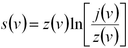
| The single scattering distribution of electrons interacting with matter is proportional to Im(−1/ε) where ε is the dielectric function which depends on the energy and the momentum transfer. Based on the cross-section for inelastic scattering, the single scattering distribution (SSD) can be expressed as, Where, For small q, ε(q,E) varies very slowly with q and thus it can be replaced by ε(E). The dielectric function ε is used to describe both single and collective excitations induced by interaction of incident electrons with materials [1]. According to Drude model [2,3], the energy loss function (ELF) for a bulk plasmon can be given by, where, Figure 4356a presents the ELF and ε1 and ε2 as a function of energy loss. The arrows show the plasmon peaks and the corresponding ε1 around their values close to 0.
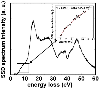
Figure 4356a. The ELF and ε1 and ε2 as a function of energy loss. [4] SSD spectra can be extracted from experimental spectra by deconvolution of elastic/quasi-elastic phonon and multiple scattering effects. For instance, this deconvolution can be done by removing multiple scattering with Fourier-log deconvolution method, and then the SSD is given by, For some materials (especially wide band gap materials), in higher energy-resolution EELS measurements, the band gap (Eg) can be determined by eye observation of the SSD spectrum that is obtained from low-loss spectra. In this case, Eg is defined as the energy corresponding to the first onset in the spectrum, for instance, 0.67 and 1.12 eV for Ge and Si respectively, in the schematic spectra in Figure 4356b.
Figure 4356b. Schematic illustration of Si and Ge SSD spectra in the low-energy range. On the other hand, the band gap can also be determined based on Bethe’s theory. In this case, the SSD spectrum is described to be proportional to the product of the joint density of states (JDOS). Here, the JDOS is given by, Therefore, Eg can be extracted by fitting the single scattering spectrum using Equations [4356d] and [4356e]. Figure 4356c shows the band gap determination of the HfO2 layer in a Si/SiO2/HfO2/poly-Ge stack by using Equation 4356d (direct band gap [Eg = 5.26 eV] for HfO2).
Figure 4356c. Band gap determination of the HfO2 layer in a Si/SiO2/HfO2/poly-Ge stack. Adapted from [5] If the SSD is known, then optical techniques such as Kramers–Kronig analysis can be applied to determine the dielectric function, reflectivity, absorption, etc. [7] For more accurate calculations, it is important to note that SSDs contain bulk plasmon-loss spectra as well as surface losses, especially when the specimens are very thin. Therefore, the SSD can be given by, ISSD(E,t) = Ib(E,t) + Is(E,t) ------------- [4356f] The surface plasmon-loss (Is) has dependence on TEM-specimen thickness only when the specimen is extremely thin (e.g. <10 nm in general). The bulk loss is given by, Ib(E,t) = t•[Ip(E) + Iint(E)+ICh(E)] ------------- [4356g] Table 4356. Electron scattering versus TEM sample thickness.
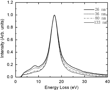
Mkhoyan et al. [6] presented SSDs obtained from experimental EELS data from silicon (Si) specimens with four different thicknesses as shown in Figure 4356d. The band gap or electronic states in the gap presented in the figure were inaccurate due to the low energy-resolution. In their measurements, the energy resolution was 0.7 eV, and the channel size 0.22 eV so that it was impossible to quantify features located below 2 eV.
Figure 4356d. SSDs obtained from experimental EELS data from Si specimens with four different thicknesses.
Adapted from [6]
It is very common that SSD is obtained by subtracting the original spectrum with a power-law fitting of the ZLP tail performed in Gatan Digital Micrograph software. If the noise in an EELS profile is large , a practical procedure to study the SSD is:
[1] Ritchie R.H. and Howie A., Phil. Mag. 36 (1977) 463.
|
 ------------------------------ [4356a]
  -- See
  ----------------------- [4356b]
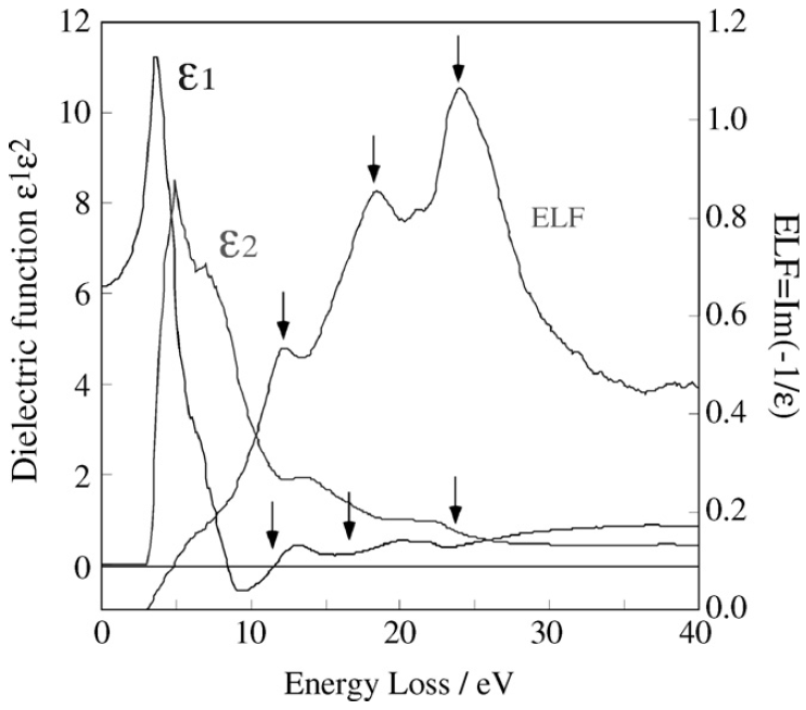
 ------------- [4356c]
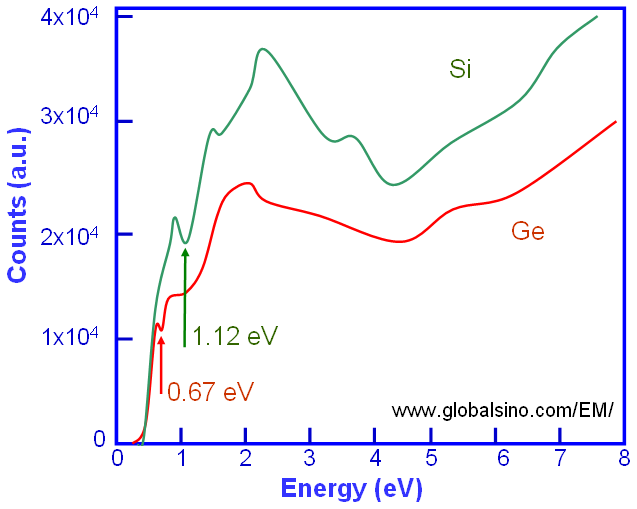
 for a direct band gap, ------------- [4356d]
 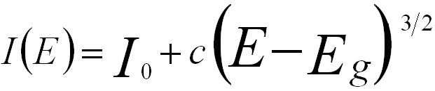 for an indirect band gap ------------- [4356e]