|
This book (Practical Electron Microscopy and Database) is a reference for TEM and SEM students, operators, engineers, technicians, managers, and researchers.
|
=================================================================================
During the collision process between incident electrons and a nucleus, if the energy (E) received by an atomic nucleus exceeds the atomic surface-binding energy Es, surface atoms can be removed in an average time, given by,
<T> ~ e/(σsJ) ------------------- [4408a]
where,
J -- The current density of the incident electron beam,
σs -- The cross section of sputtering (or called knock-on).
The sputtering cross section can be given by, [1]
 ------------------- [4408b] ------------------- [4408b]
where,
A -- The atomic mass number,
Z -- The atomic number,
E -- The energy received by an atomic nucleus due to the collision between the incident electrons and the nucleus,
E0 -- The energy of incident electrons.
Cross-sections (σ) of surface sputtering in conducting materials induced by electron irradiation is from 10-22 to 10-21 cm2.
Conventional wisdom suggests that a low operating voltage (<100 kV) in TEMs is optimal for reducing radiation damage, but the calculated profiles as a function of incident electron energy E0 in Figure 4408 demonstrate the minimum displacement cross-sections for lithium atoms in the elemental Li, lithiated graphite (LiC6) and graphite are not at low operating voltages.
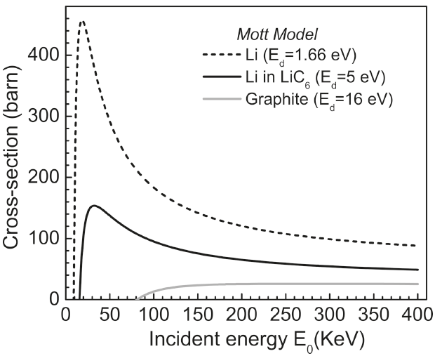
Figure 4408. The displacement cross-sections for lithium atoms in the elemental Li, lithiated graphite (LiC6) and graphite as a function of incident electron energy E0.
Ed is the displacement
energy. [2]
[1] Chadderton, L.T., 1965. Radiation Damage in Crystals, Methuen,
London.
[2] FengWang, Jason Graetz, M. Sergio Moreno, Chao Ma, LijunWu, Vyacheslav Volkov, and Yimei Zhu, Chemical Distribution and Bonding of
Lithium in Intercalated Graphite:
Identification with Optimized Electron
Energy Loss Spectroscopy, ACS Nano, 5 (2), (2011) 1190.
|