Chapter/Index: Introduction | A | B | C | D | E | F | G | H | I | J | K | L | M | N | O | P | Q | R | S | T | U | V | W | X | Y | Z | Appendix
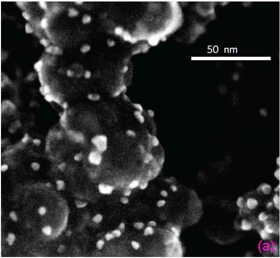
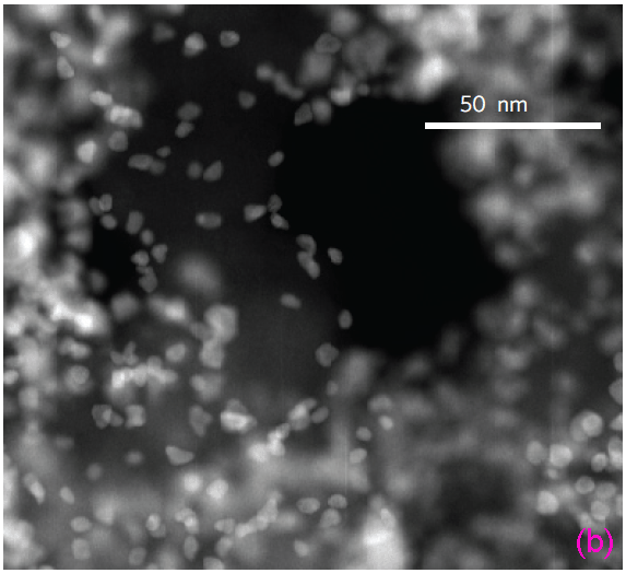
| Figure 4445 shows the contrast difference of Pd (Palladium) particles on a thin carbon film. The image (a) using SEs as well as BSEs clearly gives rich depth information, or three-dimensional (3-D) information, about the locations of the particles, while the STEM image cannot give such information.
Figure 4445. (a) SEM image of Pd nanoparticles on a carbon support obtained using SEs and BSEs; (b) STEM image obained using transmitted electrons (TEs) with an ADF detector.
Adapted from [1].
[1] Y. Zhu, H. Inada, K. Nakamura, and J. Wall, Imaging single atoms using secondary electrons with an aberration-corrected electron microscope, Nature Materials, 8 (2009) 808.
|