|
|
JEM-ARM 200F TEM
- Practical Electron Microscopy and Database -
- An Online Book -
|
|
https://www.globalsino.com/EM/
|
|
This book (Practical Electron Microscopy and Database) is a reference for TEM and SEM students, operators, engineers, technicians, managers, and researchers.
|
=================================================================================
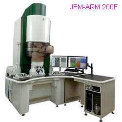
JEM-ARM 200F, a modern TEM, has been integrated with aberration correction into a super-shielded electron column that safeguards the ultrahigh-powered optics from environmental interferences. The completely new electron column design in this type of microscopes provides atomic spatial energy resolution as well as high probe currents, enabling both atom-by-atom imaging resolution and unmatched spatial resolution for atom-to-atom chemical mapping of materials, including EDS and EELS. Figure 4460 shows the resolved Si (silicon) structures by UT-SA JEOL JEM-ARM 200F. Figure 4460 (b) demonstrates that HAADF image gave at least 78 picometer spatial resolution. Clearly, these high resolution microscopes can be used for sub-atomic research.
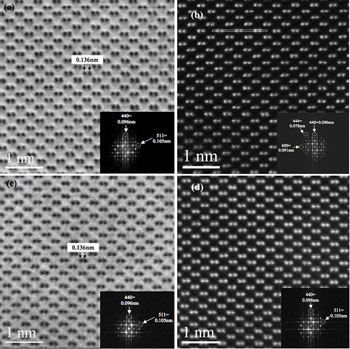
Figure 4460. (a-b) Bright field (BF) and HAADF STEM images of Si [110] taken at 200 kV on JEOL JEM-ARM 200F. The HAADF image shows spatial resolution down to 0.078 nm, while the BF image resolves spatial information < 0.1 nm. (c-d) Bright field (BF) and HAADF STEM images of Si [110] taken at 120 kV on JEOL JEM-ARM 200F. Both the HAADF and BF images show spatial resolution down to < 0.1 nm.
|
=================================================================================
The book author (Dr. Liao) welcomes your comments, suggestions, and corrections, please click here for submission. You can click How to Cite This Book to cite this book. If you let Dr. Liao know once you have cited this book, the brief information of your publication will appear on the “Times Cited” page. This appearance can help advertise your publication.
|
|