Diffraction Patterns & Crystallography of Silicon (Si)
- Practical Electron Microscopy and Database -
- An Online Book -
Electron microscopy
  Microanalysis | EM Book                                                                   https://www.globalsino.com/EM/  


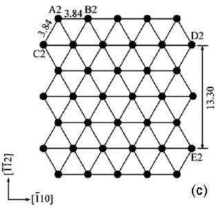
Some examples of kinematically forbidden reflections in silicon (Si) are:
        i) {222} reflections.
        ii) ±(002) reflections in the [110] orientation. In thick TEM specimen those reflections arise due to double scattering (double diffraction) by the ±(-111) and ±(1-11) reflections. They are also induced partially by the fact that the “geometrical part” of the Lorentz factor [1] may enhance their intensities since the four {111} reflections reflect the largest net-plane spacing in any <110> projection.

Figure 4489 shows the arrangement of atoms on Si (111).

Arrangement of atoms on Si (111)

Figure 4489. Arrangement of atoms on Si (111).

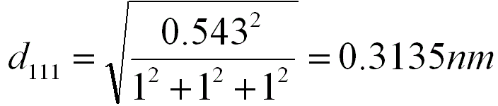
For crystals, the angles between the direct beam and diffraction spots can be calculated. For instance, the wavelength of 200-kV TEM is 0.00251 nm, and d111 for Si is 0.3135 nm, thus the angle between direct beam and Si 111 spot is given by (see page3580),

           the angle between direct beam and Si 111 spot is given by ------------------- [4489a]

Crystal Si has cubic structure. Its lattice parameter is 0.543 nm so that the (111) lattice spacing (see page3547) can be given by,

           Diffraction Patterns & Crystallography of Silicon ------------------- [4489b]

Table 4489 lists the angles (2θB) between the direct beam 000 and diffracted beams as well as the lattice spacings for Si at accelerating voltages of 200, 300 and 400 kV. The angles can be computed with the DM scripts in the table.

Table 4489. Angles (2θB) between the direct beam 000 and diffracted beams as well as the lattice spacings for a Si crystal (a = 5.431195(9) Å).
hkl
Reflection angles (1° = 17.45 mrad)
Lattice spacing (nm) Forbidden reflections
200 kV 300 kV 400 kV λ = 1.5405929 Å and T = 295.6 K
111
8.01 mrad 6.28 mrad 5.23 mrad 28.441° 0.3135  
200
          Presents in [110] orientation due to double diffraction
220
13.07 mrad 10.26 mrad 8.54 mrad 47.300° 0.1920  
311
15.33 mrad 12.03 mrad 10.02 mrad 56.120° 0.1637  
222
16.00 mrad       0.1568 Forbidden
400
18.49 mrad 14.51 mrad 12.08 mrad 69.126° 0.1358  
331
20.67 mrad 15.81 mrad 13.16 mrad 76.372° 0.1246  
422
22.65 mrad 17.77 mrad 14.80 mrad 88.025° 0.1108  
511/333
24.02 mrad 18.85 mrad 15.69 mrad 94.947° 0.1045  
440
      106.701°    
531
      114.084°    
620
      127.534°    
533
      136.880°    
622
30.66 mrad 24.07 mrad 20.03 mrad   0.0819 Forbidden
444
      158.603°    
hkl
          h, k, l are mixed odd and even; or, all even and h + k + l ≠ 4n (Or defined by h + k + l = 4n + 2)


[1] Moeck, P.; Rouvimov, S.: Structural fingerprinting of nanocrystals in the transmission electron microscope: utilizing information on projected reciprocal lattice geometry, 2D symmetry, and structure factors. In: Drug Delivery Nanoparticles Formulation and Characterization (Eds. Y. Pathak, D. Thassu), Informa, 2009 (Drugs and the Pharmaceutical Sciences, Vol. 191), pp. 270–313, (ISBN-13: 978-1-4200-7804-6).

;