| Low-resistivity polycrystalline cobalt disilicide (CoSi2) has many favorable properties, such as low bulk electrical
resistivity and good lattice match with Si (001), and has been widely used as a contact material for silicon ULSI (ultra-large scale integration) devices as the device feature size decreases [1–3]. CoSi2 has been widely used since the 0.25 µm generation. However,
the conventional process to form polycrystalline CoSi2 still suffers from serious issues such as agglomeration,
silicon consumption and leakage current. Especially, the
agglomeration issue became more critical for ULSI technology below 90 nm
because of the limitation of line width and shallow source/drain junction. The agglomeration induces large-grain CoSi2 formation and hence resistance degradation [4,5]. Epitaxial CoSi2 has been expected to resolve this problem due to its excellent thermal stability.
The crystallization process of a free-standing amorphous CoSi2 (a-CoSi2) film was found to be Co2Si → CoSi → CoSi2 [6]. Byun et al. [12] reported that the second RTA (rapid thermal annealing), which was used to convert cobalt monosilicide (CoSi) to cobalt disilicide (CoSi2), induced rapid silicon migration from silicon to cobalt monosilicide, resulting in a void. Furthermore, the transformation of the Co/Si structure to CoSi2 forms an ohmic contact but necessarily requires consumption of the Si substrate at a ratio of 1 nm Co metal consuming 3.6 nm of Si [10]. This Si consumption can induce void formation in the base Si. Note that titanium silicidation generates less silicon vacancies in the silicon substrate than by cobalt silicidation. [13]
Among the cobalt silicides, stable cobalt disilicide (CoSi2) has a fluorite (CaF2) structure with a lattice constant of 5.365 Å [7] and has low resistance (14 µΩ cm) and small lattice mismatch with (- 1.2%) Si [8]. Another compound CoSi, with a FeSi-type simple cubic structure and lattice parameter of 4.438 Å [9]. The third compound Co2Si has orthorhombic PbCl2 structure with lattice parameter of a = 7.11 Å, b = 4.92 Å and c = 3.74 Å [7]. In IC applications, a TiN capping layer is normally used to reduce an unwanted reaction of cobalt and silicon with oxygen from air and to retard the reaction between cobalt and silicon, resulting in a high quality polycrystalline cobalt disilicide. [11]
Table 4490a. Crystal parameters of Co and Co silicides. [14]
| Compound |
Crystal system |
Lattice constants (nm) |
Density
(g/cm3) |
| a |
b |
c |
| α-Co |
Cubic |
0.35446 |
|
|
8.789 |
| ε-Co |
Hexagonal |
0.25071 |
|
0.40695 |
8.871 |
| α-Co3Si |
Tetragonal |
0.8420 |
0.3738 |
0.5810 |
|
| α-Co2Si |
Orthorhombic |
0.4918 |
0.3737 |
0.7109 |
7.42 |
| CoSi |
Cubic |
0.4447 |
|
|
6.65 |
| CoSi2 |
Cubic |
0.53640 |
|
|
4.95 |
Table 4490b. Properties of Co2Si, CoSi, and CoSi2 materials.
Properties |
Co2Si |
CoSi |
CoSi2 |
Thin film
resistivity
(μΩ − cm) |
~70 |
100-150 |
14-25 |
Melting point
(°C) |
|
|
1325 |
Thermal expansion (ppm/°C) |
|
|
~10 |
Sintering temperature
(°C) |
300-500 |
400-600 |
600-800 |
Stable on
Si up to
(°C) |
|
|
~950 |
Reaction
with Al at
(°C) |
|
|
400 |
nm of Si
consumed
per nm of
metal |
0.91 |
1.82 |
3.64 (High Si consumption results in problem in scaling junctions: Not scalable to ultrashallow junctions) |
nm of
resulting
silicide
per nm of
metal |
1.47 |
2.02 |
3.52 |
Si consumption (nm Si/nm Silicide) |
|
|
1.03 |
Barrier
height to
n-Si (eV) |
|
|
0.65 |
Table 4490c. Comparison of the properties of CoSi2 and TiSi2.
Property |
CoSi2 |
TiSi2 |
Resistivity |
10-25 µΩ/cm |
12-24 µΩ/cm |
Metal-dopant compound formation |
No |
Yes |
Thermal stability on single crystalline Si |
Good
|
|
Thermal stability on undoped poly-Si
|
|
|
Thermal expansion |
~10 ppm/°C |
12 ppm/°C |
Mechanical stress
|
(8-10) x 109 dyne/cm2
|
(2-2.25) x 1010 dyne/cm2 |
Si consumption (nm Si/nm Silicide) |
1.03 |
0.904 |
Reaction temperature with SiO2 |
> 1000 °C
|
700 °C |
Dominant diffusion species during silicide formation |
Co |
Si |
Sheet resistance control
|
Good |
Poor |
Resistivity to dry/wet etching |
Good
|
Poor |
Native oxide consumption
|
Poor
|
Good |
Thermal stability in the Al/silicide/Si system |
Poor |
Poor |
Lattice match with Si
|
Good
|
Poor |
Melting point |
1325 °C |
1540 °C |
Figure 4490 shows phase diagram of cobalt Silicides.
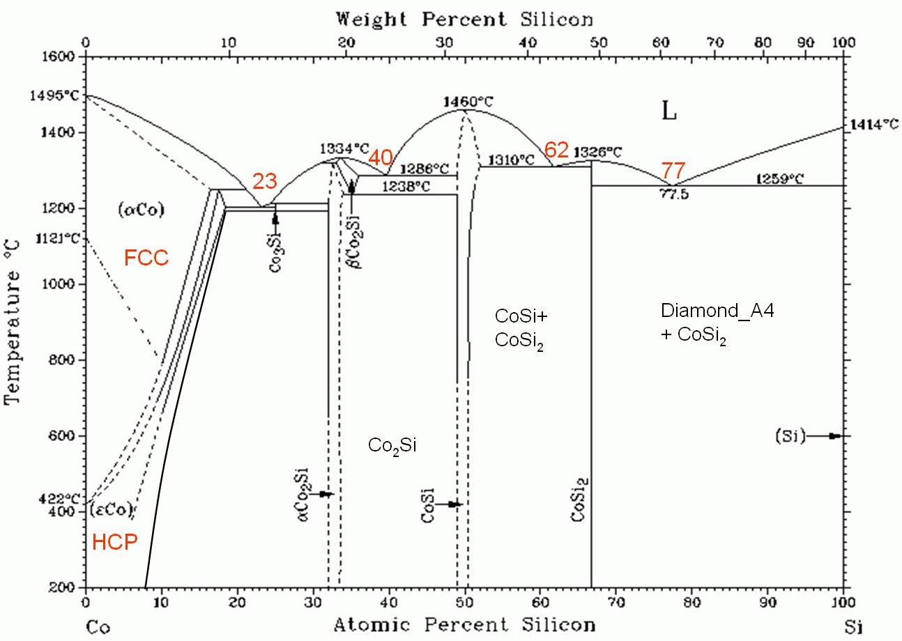
Figure 4490. Phase diagram of cobalt Silicides.
[1] D.J. Yang, Q. Zhang, G. Chen, IEEE Trans. Electron Devices 54 (2007) 2730.
[2] C. Fitz, M. Goldbach, A. Dupont, S. Schmidbauer, Microelectron. Eng. 82 (2005)
460.
[3] K. Kawamura, S. Inagaki, T. Saiki, R. Nakamura, Y. Kataoka, M. Kase, Jpn. J. Appl.
Phys. 46 (2007) 7268.
[4] S. Vaidya, S.P. Murarka, T.T. Sheng, J. Appl. Phys. 58 (1985)
971.
[5] C.Y. Ting, F.M. d_Heurle, S.S. Iyer, P.M. Fryer, J. Electrochem. Soc.
133 (1986) 2621.
[6] J.Y. Shim, S.W. Park, H.K. Baik, Silicide formation in cobalt/amorphous silicon,
amorphous Co–Si and bias-induced Co–Si films, Thin Solid Films 292 (1997)
31–39.
[7] F. Zeng, X. Xiong, B. Huang, Cobalt silicide formations and magnetic properties of laser ablated Co(Cr) thin films, Intermetallics 18 (2010) 306–311.
[8] He Y, Feng JY, Li WZ. Effect of substrate temperature on CoSi2 formation by
a metal vapor vacuum arc ion source. J Cryst Growth 264, (2004) 266–70.
[9] He G, Jiao LF, Yuan HT, Zhang YY, Wang YJ. Preparation and electrochemical
hydrogen storage property of alloy CoSi. Electrochem Commun 8 (2006) 1633–8.
[10] Zhang S L and Ostling M 2003 Crit. Rev. Solid State Mater.
Sci. 28 1–129.
[11] D.-K. Sohn, J.-S. Park, B.-H. Lee, J.-U. Bae, J.-S. Byun, and J.-J. Kim,
Appl. Phys. Lett. 73, 2302 (1998).
[12] J. S. Byun, J. M. S., K. Y. Youn, H. H., J. W. Park, and J. J. Kim, J. Electrochem. Soc. 143, L56 (1996).
[13] S. B. Herner, K. S. Jones, H.-J. Gossmann, J. M. Poate, and H. S. Luftman,
Appl. Phys. Lett. 68, 1687 (1996).
[14] K. Maex, M. Van Rossum, A. Reader [Crystal structure of TM silicides,
in Properties of Metal Silicides Ed. K. Maex, M. Van Rossum, EMIS
Datareviews Series No. 14 (IEE, UK, 1995)]
|
