X-ray Detectors & EDS Comparisons in SEM/TEM/STEM - Practical Electron Microscopy and Database - - An Online Book - |
||||||||||||||||||||||||||||||||||||||||||||||||||||||||||||||||||||||||||||||||||||||||||||||||||||||||||||||
| Microanalysis | EM Book https://www.globalsino.com/EM/ | ||||||||||||||||||||||||||||||||||||||||||||||||||||||||||||||||||||||||||||||||||||||||||||||||||||||||||||||
Table 4532a lists the properties of common X-ray detectors.
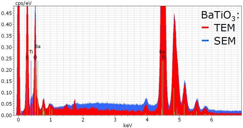
The X-ray detector crystal is behind the EDS detector window, and is commonly made up of a lithium (Li) impregnated silicon (Si) wafer that is maintained at cold temperatures by liquid nitrogen (N2) stored in a Dewar located on the outside of the microscope. The main requirements of EDS detectors for EMs are: The background counts in TEM-EDS are much lower than those in SEM-EDS spectrum. Due to the high background counts in SEM-EDS, an artificial carbon (C) peak is always visible and thus a value of more than 2% carbon is normally measured even though there is no carbon in the specimen. This artefact is due to the window in the detector. The EDS windows are normally SATW windows and their material has a specific transmission profile with a strong absorption edge just above but very close to the C X-ray energy, resulting in an artificial peak at the C energy position. Therefore, it is the strong absorption of the background (continuum) X-rays that produces the artefact peak. Note that SATW detector windows are AP* ultrathin polymer windows manufactured by Moxtek and are almost supplied by all EDS detector companies. However, a TEM-EDS spectrum taken from the same specimen materials does not show such a artefact peak at the carbon energy because the spectrum consists mostly of characteristic X-rays. Table 4532b lists the main reasons why EDS measurements in low-energy SEM or high-energy (S)TEM have not replaced each other. Table 4532b. Comparison between the EDS measurements in low-energy SEM and high-energy (S)TEM*.
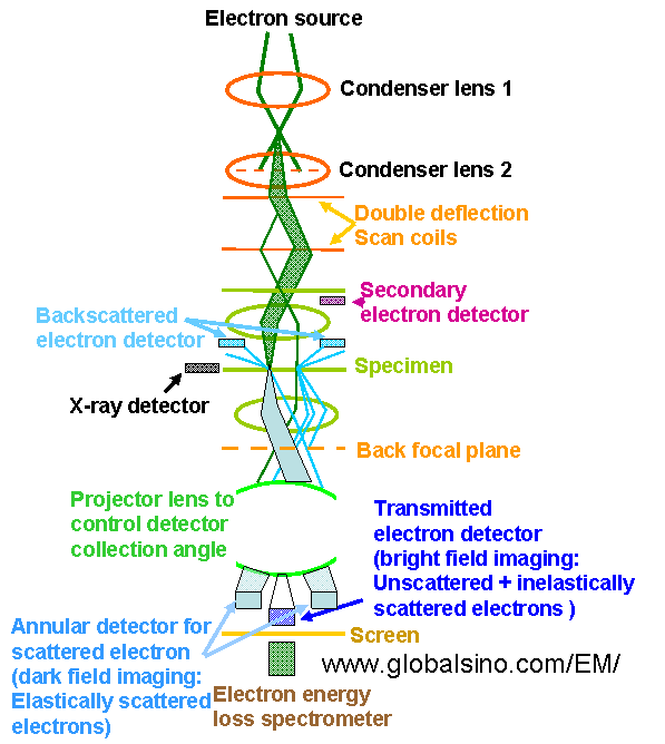
*Note: To have high spatial resolution, EDS measurement in (S)TEM has to be performed in STEM mode. Note that the use of a large convergence angle, as occurs in the STEM mode with a focused probe minimizes the problem of channeling enhanced X-ray emission. The schematics in Figure 4532 shows the electron optical column in a modern analytical electron microscope operated in STEM mode.
Figure 4532. Schematics of the electron optical column in a modern
[1] Ralf Terborg, Bruker.
|
|
|||||||||||||||||||||||||||||||||||||||||||||||||||||||||||||||||||||||||||||||||||||||||||||||||||||||||||||