|
|
Electron Probe X-ray Microanalyzer (EPMA)
- Practical Electron Microscopy and Database -
- An Online Book -
|
|
https://www.globalsino.com/EM/
|
|
This book (Practical Electron Microscopy and Database) is a reference for TEM and SEM students, operators, engineers, technicians, managers, and researchers.
|
=================================================================================
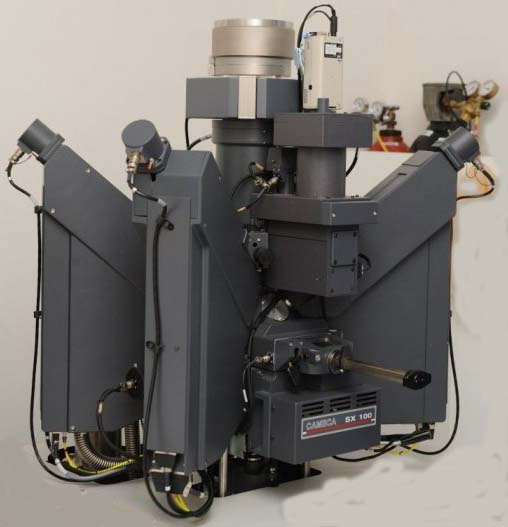 |
Figure 4609. Example of electron probe X-ray microanalyzer (EPMA): CAMECA SX-100 equipped with four crystal spectrometers, BSE and SEM detectors
|
The principle of electron probe X-ray microanalyzer (EPMA) is that a focused accelerating electron beam interacts with at an interesting point on the surface of a relatively flat sample in a micro-volume, generating the X-ray spectrum and providing qualitative and quantitative elemental microanalysis. The energy of incident beams is typical from 5 to 30 keV. EPMAs can normally be computer-controlled and equipped with both Energy Dispersive (EDS or called EDX) and Wavelength Dispersive X-Ray Spectrometers (WDS) as well as both Scanning Electron Microscope (SEM) and Backscattered Electron Imaging (BSE) as shown in Figure 4609. For instance, some EDS/WDS combined system can simultaneously analyze up to 13 or more elements (e.g. 5 WDSs and 8 EDSs).
WDS/EDS combined microanalyzers can provide higher detection sensitivity for trace elements, higher accuracy of quantitative analysis, higher spatial for adjacent X-rays, and higher accuracy of quantitative analysis for light elements. The sensitivity of this technique is normally at the level from 50 to 1000 ppm. Accurate quantification can be done down to volumes of a few cubic micrometers. High spatial resolution, e..g for smaller particles, can also be obtained at considerably lower levels of accuracy. The major applications of this technique are in the fields of geochemistry, mineralogy, physical metallurgy, nuclear metallurgy, materials science including glass, ceramics, superconductors, cements, microelectronics, biochemistry, and so on. The most precise and accurate micro-analysis by this technique can be used for determination of thickness and elemental composition down to nm thick layers, and analysis of all elements from beryllium to uranium
|
=================================================================================
The book author (Dr. Liao) welcomes your comments, suggestions, and corrections, please click here for submission. You can click How to Cite This Book to cite this book. If you let Dr. Liao know once you have cited this book, the brief information of your publication will appear on the “Times Cited” page.
|
|