Energy Resolution of EDS Technique - Practical Electron Microscopy and Database - - An Online Book - |
|||||||||||||||||||||||||||||||||
| Microanalysis | EM Book https://www.globalsino.com/EM/ | |||||||||||||||||||||||||||||||||
In general, EDS has poor energy resolution of the peaks. The widths of X-ray peaks in EDS measurements are determined by the energy resolution of the detector, but not by the atoms in the specimen. A typical EDS peak is about 100 times the natural peak width, which is limited by the statistics of electron-hole pair production and electronic noise, resulting in severe peak overlaps. In EDS investigations, good energy resolution is important for easy isolation, identification, and measurement of peaks. The spectral resolution of the EDS system is the main indicator of the quality of the X-ray sensor, amplifier, and pulse processor electronics. Spectral energy resolution is a function of the electronic shaping time that also determines storage throughput and dead time. On the other hand, both the detector and field-effect transistor (FET) of the first stage of preamplifier are cooled to get an optimum of energy-resolution. The energy resolution R of an EDS detector can be defined by, R2 = P2 + I2 + X2 ----------------------------- [4654a] where, I = 2.35 (FεE)1/2 ----------------------------- [4654b] where, P = (5.5 F ε E + N2 )1/2 ----------------------------- [4654c] For a given sensor material in the detector and a given x-ray energy, the “F ε E” term is a constant so that reducing the electronic noise (N) is the main method to improve the spectral energy resolution. The electronic noise is mathematically given by, The first term on the right side of Equation 4654d represents the thermal noise, the second term the 1/f noise, and the third term the leakage current. The characteristics of various EDS detectors is listed on a table on page4655. The natural line width of the emitted X-rays (e.g. Mn Kα line) in EMs (electron microscopes) is only a few eV but the line widths obtained with EDS systems are normally larger than 100 eV. The natural energy distribution of the characteristic X-rays of a single line is well described by the Lorentzian probability distribution instead of Gaussian shape obtained by the energy-dispersive detectors. The electronic noise in the EDS system introduces the peak broadening that is a major source causing the difference between the EDS-detected and natural energy resolutions. For instance, the typical resolution of a Si-Li EDS detector is ~130 eV due to the statistics of electron-hole pair production and electronic noise in the processing chain. The width of the electronic noise is also described as the ‘point-spread function’ of the detector (See Equation 4654a). The resolution of a detector can be practically evaluated by measuring the peak widths of different elements. The typical energy resolution for X-ray photons from most elements in EDS is of on the order of 135 - 150 eV. Table 4654a lists the practical energy resolutions (full width at half maximum of the peaks) of various elements. These parameters can be applied to evaluate the freshly installed EDS system. Table 4654a. Practical energy resolutions (FWHM of the peaks) of various elements in EDS.
No chemical-state information (with energy separation of < 10 eV) can be extracted in EDS measurements because of its poor energy resolution. Due to the same reason, there are mainly two classes of typical problems that are caused by peak overlaps: Table 4654b shows the effect of processing time on spectral parameters. The peak width determines the energy resolution of the spectrum. Based on the table, in practical EDS measurements, the processing time needs to be adjusted for a suitable energy resolution. Table 4654b. Effect of processing time on spectral parameters.
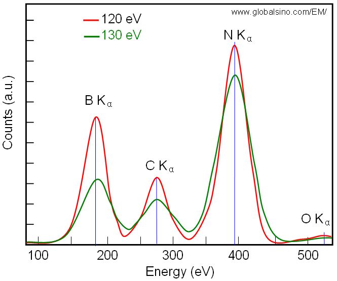
Figure 4654 shows two schematic spectra obtained from two EDS detectors with energy resolutions at Mn Kα 120 eV and 130 eV, respectively. It is clear that higher spectrum peak can be obtained with better resolution. Consequently, the higher peak improves the peak-to-background ratio and facilitates the spectrum deconvolution.
|
|
||||||||||||||||||||||||||||||||
 ----- [4654d]