Chapter/Index: Introduction | A | B | C | D | E | F | G | H | I | J | K | L | M | N | O | P | Q | R | S | T | U | V | W | X | Y | Z | Appendix
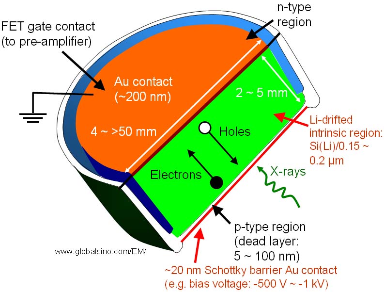
| The X-ray signal in electron microscopes (EMs) is often collected by compact solid state detectors based on lithium-drifted silicon, Si (Li), diodes as shown in Figure 4655a. In the Si(Li) detectors, a bias is applied across the crystal. The diode consists of a Si crystal with lithium atoms diffused, or drifted, from one end into the matrix. The lithium atoms are used to compensate the low concentration of grown-in impurity atoms by neutralizing them. In the diffusion process, the central core of the Si crystal becomes intrinsic, but the end away from the lithium remains p-type and the lithium end is n-type, resulting in a p-i-n diode. The crystal is maintained at low temperatures in order to prevent diffusion of Li from the intrinsic region into the Li-free regions, especially when there is a voltage across the detector.
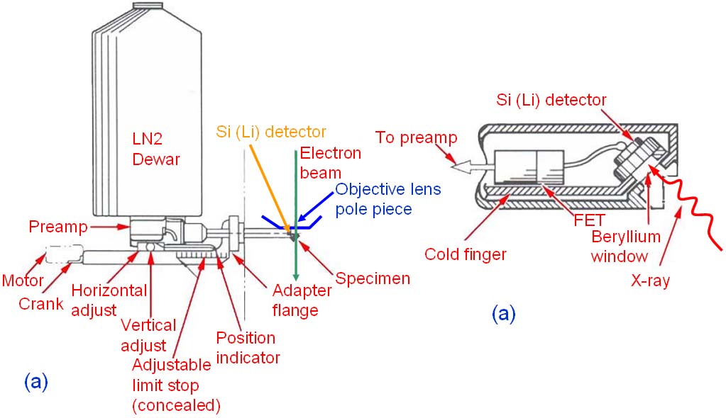
Figure 4655a. Schematic illustration of typical lithium-drifted silicon detectors. Ohmic or Schottky contacts formed by gold (Au) are normally made on both sides of the semiconducting device. A reverse electrical potential of 500-1000 volts is applied to the thin Au layers. When an X-ray photon from the specimen enters the intrinsic region of the detector through the p-type end, there is a high probability that it will ionize a Si atom through the photoelectric effect. This leads to an X ray or an Auger electron, resulting in a number of electron-hole pairs in the Si (Li), i.e. one pair per 3.8 eV of energy from X-ray photons. For example, a 5-keV X ray absorbed by the Si atoms will produce about 1315 electron-hole pairs or a charge of about 2.1 x 10⁻¹³ Coulombs. Both charge carriers move freely through the lattice and are drawn to the detector contacts by the reverse electrical potential. Therefore, the charged pulses can be measured. The signal is subsequently amplified by the low-nose FET devices before being stored in the appropriate energy channel of the multi-channel analyzer (MCA). In this case, the received pulse is used to charge a capacitor that is discharged through a constant current source attached to an address clock typically operating at 50 MHz. The time to discharge the capacitor to 0 V depends on the pulse amplitude, and thus on the X-ray energy. The 50-MHz clock generates a binary number in one of the 1024 channels typically used by the MCA and matches the discharge time. Once the channels in the MCA are calibrated in energy, the collection of X-ray pulses may be displayed on a cathode ray tube (CRT) or recorded on PC as an energy histogram. The p and n regions are called “dead layers” because more of the electron-hole pairs created in these regions do not contribute to the spectra observed. The X-ray photon is sorted by energy, hence the alternative names for X-ray fluorescence analysis are Energy Dispersive X-ray Spectroscopy (EDS or EDX). The Si (Li) diodes are operated at liquid nitrogen temperature. The main functions of the LN2 device in EDS systems in EMs are to reduce thermal e-h pair, prevent the Li atoms from diffusing, and reduce noise in the FET preamplifier. To prevent condensation or contamination build up on the cooled silicon crystal surface, the detector is usually isolated from the microscope column by a thick beryllium `window'. However, the window is transparent only to X-rays of energy greater than about 1 keV. Low-energy, or soft, X rays are strongly absorbed by the Be window, limiting the analysis range of these detectors to the elements having atomic number Z≥11. Figure 4655b shows the schematic illustration of a retractable EDS detector and its associated preamplifier electronics, and the detail of Si (Li) mounting assembly.
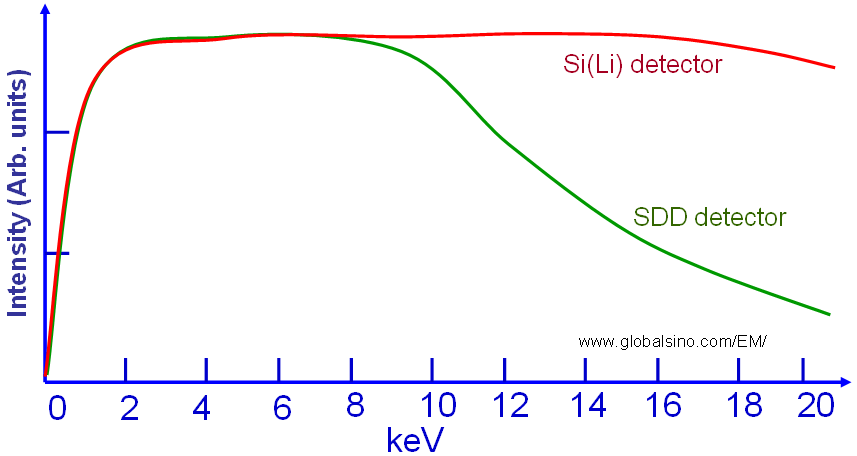
Figure 4655c shows the comparison between the detection efficiencies of Si(Li) and SDD detectors. Si(Li) detectors are more sensitive to high-energy x-rays because of the greater thickness of the Si(Li) sensors, while the SDD detectors are less sensitive because the high-energy X-rays easily penetrates through the “thinner” SDD sensor.
Figure 4655c. The comparison between the detection efficiencies of Si(Li) and SDD detectors. Furthermore, page2527 lists the comparison of various X-ray spectrometers, including lithium-drifted silicon (Si(Li)), Si-drift detectors (SDD), intrinsic-Ge (IG), wavelength dispersive X-ray spectroscopy (WDXRF/WDS), and Bolometer detectors. The typical energy resolution of a Si-Li EDS detector is ~130 eV due to the statistics of electron-hole pair production and electronic noise in the processing chain.
|