Chapter/Index: Introduction | A | B | C | D | E | F | G | H | I | J | K | L | M | N | O | P | Q | R | S | T | U | V | W | X | Y | Z | Appendix
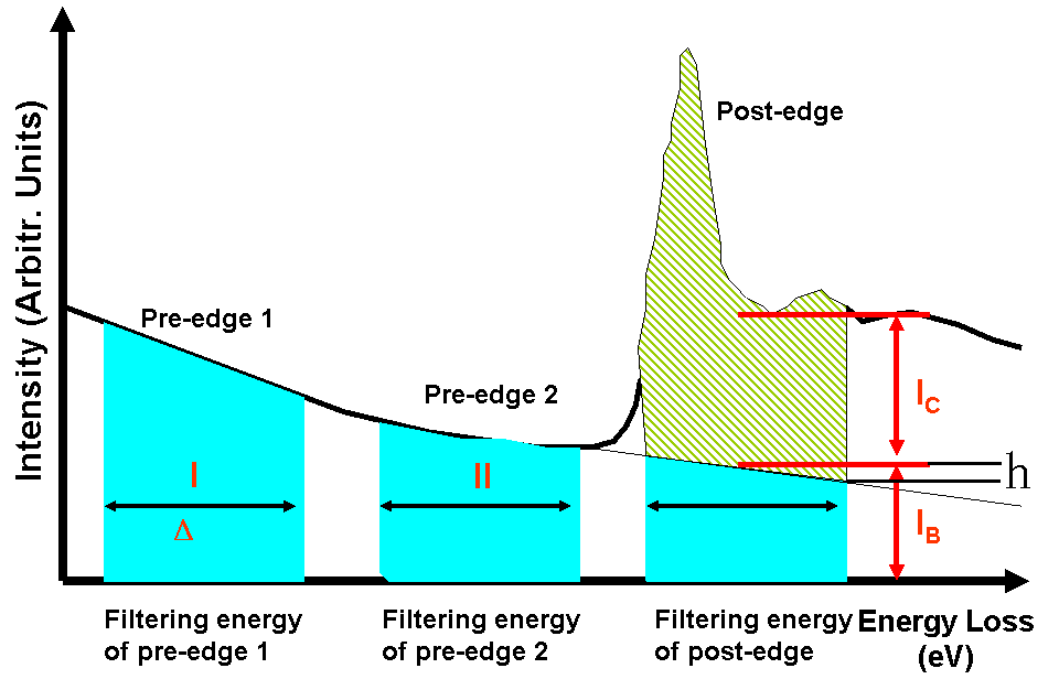
| In practice, the most straightforward method for background subtraction in EFTEM (Energy Filtered Transmission Electron Microscopy) elemental mapping and EELS (Electron Energy Loss Spectroscopy) elemental quantification is three-window method. In this technique, the background can be calculated from two pre-edge (pre-edge 1 and pre-edge 2) images in front of the ionization- (core-) edge assuming a inverse power law dependence at each pixel in the image, i.e. a model of the form A x E-r [1 - 2]. The energies of the two pre-edges are different. However, the energy widths for the three windows are normally selected at the same value (Δ) as shown in Figure 4719a. The fitting constants A and r can be found from the two pre-edge windows. With the two coefficients the background IB at post edge position can be computed and subtracted from the total signal, giving the net core-loss signal IC for an energy window (Δ). The extrapolated background image is applied to the post-edge image to give an accurate elemental map, in which changes in background shape are taken into account. After background subtraction the remaining core-loss intensity image (elemental map) or spectrum displays the spatial distribution of the element or quantification within the interesting area or point. For EFTEM, the present pixel intensities in the map are directly linked to the number of atoms of a specific element and can be converted into real concentration maps [3 - 6]. The subtraction of background in three-window method is discussed in the Section of Signal-to-Noise Ratio (SNR) in the EELS Spectrum.
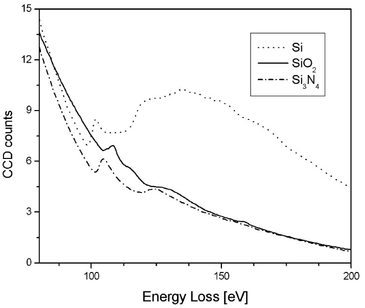
Figure 4719a. Schematic of three-window methods for EFTEM elemental mapping and EELS elemental quantification. Figure 4719b shows the Si L2,3 EEL spectra of Si, SiO2 and Si3N4. The positions of the edge onsets clearly indicate chemical shifts and differences in ELNES present. In Figure 4719b, for pure Si, the ELNES shows a first peak at 101.5 eV followed by a small plateau between 105 and 114 eV, and a very broad peak with the maximum at 135 eV. The SiO2 ELNES has a strong peak at 108.5 eV, which is also followed by a small plateau between 112 and 116 eV. However, the second peak located at 128 eV is far less intensive than the one for Si. An additional small peak presents at 161 eV. The ELNES of Si3N4 is very similar to the SiO2 ELNES. The two main peaks are located at 105 and 124.5 eV.
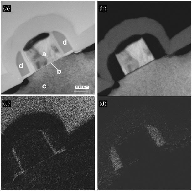
Figure 4719b. Si L2,3 EEL spectra of Si, SiO2 and Si3N4. [7] In order to distinguish different compounds containing a specific element, e.g. silicon in pure Si, SiO2 and Si3N4, the positions of the energy windows (in three-window method) and respective slit widths have to be chosen according to the ELNES as mentioned above. Table 4719 shows the optimized imaging filter settings in three-window EFTEM mode for Si, SiO2 and Si3N4. For Si mapping in SiO2 the post-edge window was placed above the second peak at 143 eV (See Table 4719). The two pre-edge windows were placed in the small plateau region between the first (110 eV) and the second (125 eV) peaks. The optimal slit width was found to be 5 eV. The filter settings for Si3N4 were determined in a similar way by considering the shift of the Si L2,3 spectrum towards lower energy loss energies. Therefore the pre-edge windows were placed at 107 and 110 eV. The post-edge window was placed at 114 eV in order to avoid interference with Si and SiO2 signals. A slit width of 3 eV was used. Those settings were used to take Si images in a MOSFET structure as shown in Figure 4719c. Note that in those images, SiO2 and Si3N4 can be distinguished without mapping O and N elements. It is clearly shown that the polycrystalline Si gate (a) is separated by a thin dielectric layer (b) from the single crystalline Si (c). The spacers (d) consisting of two different types of material can be seen on both sides of the gate. Between the polycrystalline gate and the single crystalline Si, the gate oxide layer is also seen clearly. The spacers consist of two layers, namely a thin SiO2 layer and a thicker Si3N4 layer. Note that the bright contrast at the top of image (c) can be an artifact because of the signal of some elements overlapping the Si energy windows of SiO2.
Figure 4719c. TEM bright field image and ELNES Si maps of the MOSFET structure: (a) TEM bright field image; (b) Si map; (c) Si map in SiO2; (d) Si map in Si3N4.
[7]
Table 4719. The imaging filter settings of EFTEM for Si, SiO2 and Si3N4. [7]
Note that the selection of the energy windows affects the accuracy of mapping and quantification significantly in EELS measurements.
[1] Jeanguillaume C., Trebbia P., Colliex C., 1978. About the use of electron
energy-loss spectroscopy for chemical mapping of thin foils with high
|