=================================================================================
With a TEM specimen in the electron path, the first peak in EELS spectrum occurs at 0 eV, also called zero-loss or “elastic” peak as shown in Figure 4775a. This is the most intense (predominant) peak, especially for a very thin specimen. It represents energy spread and stability of the electron gun, electrons that undergo inelastic scattering without suffering significant energy loss (e.g. electrons scattered elastically and those that excite phonons) but which might have been scattered elastically through interaction with atomic nuclei. The zero-loss peak also includes electrons that are unscattered. That means the recorded electrons in the zero loss peak have passed the sample without measurable energy loss or with energy changes too small to be measurable from phonon excitations (a few 10 meV) within scattering angle of ~ 50 mrad. However, most electrons in the zero-loss peak are forward scattered in a relatively narrow cone within a few mrad of the optic axis and consists of the 000 spot in the diffraction pattern, i.e. the direct beam. The width of the zero-loss peak, typically 0.2 – 2 eV, reflects mainly the energy distribution of the electron source. However, it is important to note that the corresponding electron waves undergo a phase change, which is only detectable by holography or high-resolution imaging. For thin TEM samples, most electrons do not participate in an inelastic scattering event so that the zero loss peaks are normally very intense.
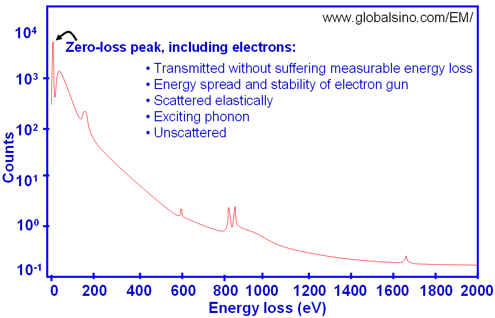
Figure 4775a. Zero-loss or “elastic” peak in EELS profile on a logarithmic scale.
To evaluate an electron source, the ZLP is normally determined without any TEM specimen. Zero-loss peaks (ZLPs) in EELS can be measured without and with a specimen. For instance, Figure 4775b shows the ZLPs of a CFEG (cold field emission gun) [2] at various emission currents as well as the monochromatized ZLP [3] in logarithmic vertical scale. The inset lists the extraction voltages V1, probe currents Ip and the FWHMs (full width at half maximum) of the ZLPs. Note that the FWHMs quantify the energy spread. In general, the lower extraction voltage and probe current gives smaller FWHMs of the ZLPs, meaning that the higher energy resolution can be obtained, while the one with a monochromator still has the lowest FWHM.
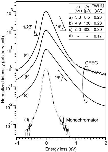
Figure 4775b. ZLPs of CFEG under various emission conditions as well as the monochromatized ZLP.
Adapted from [2]
The Fowler-Nordheim (F-N) energy distribution of emitted electrons includes two distinct regions [4]: a low energy Fermi tail and a high energy tunnelling tail. In other words, the energy distribution of emitted electrons is the product of the Fermi–Dirac distribution function ln(1+eΔ/kT) and the tunneling probability exp[-b(φ+Δ)3/2/F],
which produce the Fermi tail and the tunneling tail,
respectively, and causes beam energy-broadening in field emission guns. The low energy Fermi tail is a property of the Fermi surface of the tip material (e.g. tungesten) and is independent of the extraction voltage. The left side of the CFEG’s ZLP is comparable to that of the monochromator. The slope of the high energy tunnelling tail is determined by the field strength. In this case, it is difficult to determine the onset of the inelastic scattering within a low-loss spectrum because the tunneling tail induces a strong background. Therefore, the monochromator has an advantage in the measurement of small bandgaps (e.g. ≤1 eV).
The complete ZLP without any specimen is formed from a convolution of the energy distribution from the emission source (e.g. Fowler-Nordheim distribution for field emission sources), the point spread function (PSF) from the spectrometer and a narrow Gaussian to represent the drift of the high voltage supply.
In practice, depending on the characteristics of the electron source, the ZLP tails may spread up to 10 eV or more away from the nominal energy of the incident electrons.
Sasaki et al. [1] used Cs correctors to correct their lower-voltage STEM/TEM system. For the Cs corrected microscope, Figure 4775c shows the energy spreads, determined from the FWHM (full width at half maximum) of the zero-loss peaks are 0.30 and 0.27 eV at 30 and 60 kV, respectively, with an exposure time of 0.05 s.
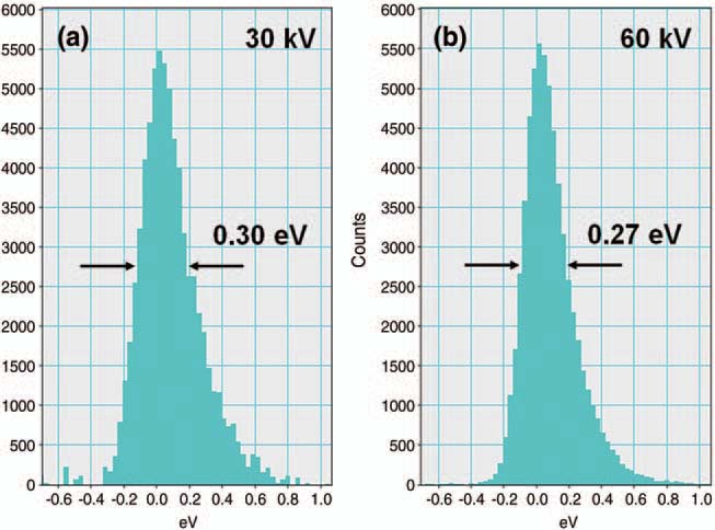
Figure 4775c. Zero-loss peaks of EELS spectra measured at (a) 30 kV and (b) 60 kV in the Cs corrected microscope. [1]
The energy changes of incident electrons associated with thermal diffuse scattering
(TDS) are of the order of kT ≈ 0.05 eV and are too small to be measured by EELS tools because most EELS instruments have typical energy resolution of >0.1 eV.
Figure 4775d shows the schematic illustration of laterally resolved EELS across the multi-layers in the specimen. The horizontal stripes in Figure 4775d (a) represent the multi-layers in the TEM specimen. At high dispersion (a low eV/channel value), the curvature of the zero loss (ZL) peak on the CCD indicates the non-isochromaticity of the filter, while at low dispersion the curvature of the ZL is hardly visible.
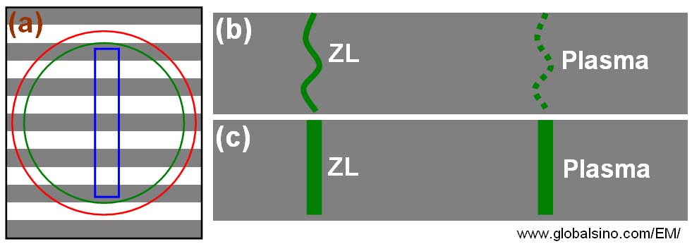
Figure 4775d. Schematic illustration of the laterally resolved EELS across the multi-layers in the specimen. (a) The slit aperture (in blue) across the interface of the multi-layers. The red (bigger) and green (smaller) circles represent the illumination area by the electron beam and the round spectrometer entrance aperture, respectively. (b) At high dispersion (a low eV/channel value), the curvature of the zero loss (ZL) peak on the CCD indicates the non-isochromaticity of the filter. (c) At low dispersion the curvature of the ZL is hardly visible.
[1] Takeo Sasaki, Hidetaka Sawada, Fumio Hosokawa, Yuji Kohno, Takeshi Tomita, Toshikatsu Kaneyama, Yukihito Kondo, Koji Kimoto, Yuta Sato, and Kazu Suenaga, Performance of low-voltage STEM/TEM with delta corrector and cold field emission gun, Journal of Electron Microscopy 59(Supplement): S7–S13 (2010).
[2] Koji Kimoto, Kazuo Ishizuka, Toru Asaka, Takuro Nagai, Yoshio Matsui, 0.23 eV energy resolution obtained using a cold field-emission gun and a streak imaging technique, Micron 36 (2005) 465–469.
[3] Kothleitner, G., Hofer, F., 2003. EELS performance measurements on a new
high energy resolution imaging filter. Micron 34, 211–218.
[4] Kimoto, K. et al. 0.23eV energy resolution obtained using a cold field-emission gun and a streak imaging technique. Micron 36, 465-469 (2005).
|