=================================================================================
Secondary electron yield at SEM sample surfaces
Secondary electron emission (SEE) is a common phenomenon induced by high energy electrons interacting with a specimen. Only the SE yield of top surfaces of SEM samples are referred if it is not specified to TEM thin films (see below). Because the specimen is very thick in SEM observation, almost each incident electron can produce several secondary electrons (SEs). The coefficient of emission, or called as yield, of secondary electrons can be given by δ = iδ/ii. Here, iδ is the total emission current and ii is the current of incident electron beam. It means that the SE yield (δ) is the ratio between the SE current and the primary electron current. In other words, SE yield (δ) can be defined as the number of secondary electrons emitted per incident electron and can be either less than or greater than one. δ depends on the energy (E0) of incident electron beam, angle of incident electron beam, chemical composition, and state of the irradiated sample’s surface.
In many cases, the conduction-electron density in metals is high, the SEs have a low probability of escaping the surface of materials; while the concentration of conduction electrons in dielectrics is low, the probability of the escape of SEs is greater.
The relative yields of SEs between different materials can change depending on energy of incident electron beam. Figure 4835a shows the yields of secondary and backscattered electrons, and their sum as a function of the accelerating energy of incident electrons in an electron microscope.
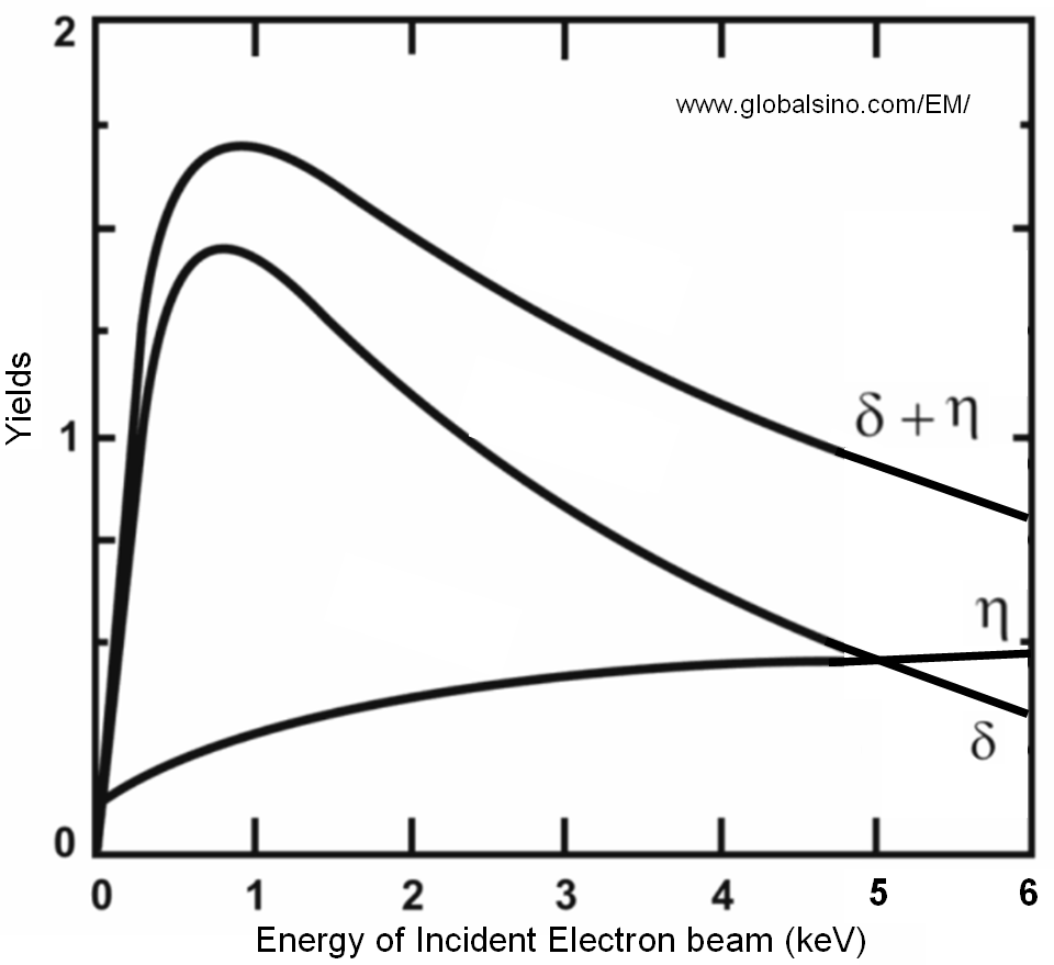
| Figure 4835a. Yields of secondary and backscattered electrons, and their sum as a function of the accelerating energy of incident electrons in an electron microscope. |
Figure 4835b shows experimental and theoretical secondary electron yields from quartz [1] and platinum [2]. The theoretical modeling was performed by constant loss model [3,4] and parabolic model [5]. In the modeling, the researchers considered some factors such as magnitude for SE attenuation length, s, and SE escape probability, A, of the materials of interest. It is very interesting that the crossing of yield curves, δ(E0), is at around E0 = 2 keV. This crossing suggests a contrast change as well as a contrast reversal in the range of incident beam energy from ~1 to ~4 keV as shown by the arrows in the figure.
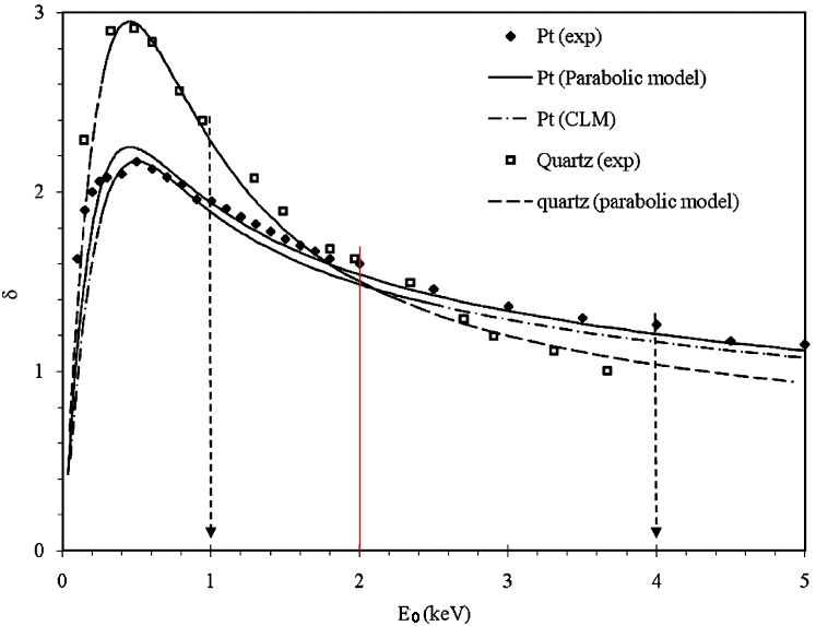
Figure 4835b. Secondary yield curves δf(E0) of Pt and quartz. “exp” represents experimental data. The other ones are simulated data.
It is well-known that the probability of secondary electron escape also depends on the height of the potential barrier on the sample surface. As a result, in a number of nonmetallic substances (oxides of alkaline-earth metals; alkali-halide compounds), their yield is much higher than other materials, e.g. as shown in Figure 4835c.
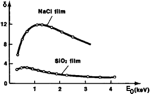
Figure 4835c. Dependence of the coefficient of secondary electron emission of NaCl and SiO2 on the energy of the incident electron beam.
In Figures 4835b - 4835d, we can notice that σ at first increases with an increase of the energy E0 of the incident electron beam, which takes place until the excitation of the electrons of the solid occurs near the surface at a distance of their path length. Upon further increase of E0, the total number of excited electrons continues to increase, but most of them originate at a greater depth, and the number of SEs that escape decreases.
Figure 4835d. Dependence of the coefficient of secondary electron emission of Pt and Mo on the energy of the incident electron beam.
Furthermore, many other factors can also enhance SE emission. For instance, SE emission can be enhanced by electrostatic fields and ultrahigh-frequency electrical fields as well as the porosity of materials. In general, the energy dependence on incident electrons shows a maximum δm = 0.35 – 1.6 for metals and 1 – 10 for insulators at energies of Em = 100 – 800 eV and 300 – 2000 eV, respectively. [6] Here, Em is the energy of incident electrons at which the maximum δm locates.
The secondary-electron yield δ is proportional to:
i) the Bethe loss
|dEm/dx| in the surface layer.
ii) the path length tSE·secφ inside
the exit depth. Here, φ is the angle between the incident direction and the surface
normal.
Physically, the SE yield (δ) can be given by,
 ------------- [4835a] ------------- [4835a]
where n(z, E0)dz -- Number of SE generated by
incident energy E0 in the layer of thickness dz at a depth z
below the surface.
λ -- Mean free path (MFP)
Pe -- Escape probability (= B)
The secondary electron yield, δ, can also be composed of the contributions from the primary electrons and the reflected (backscattered) electrons, [9]
δ = δPE + δBE = δPE(1 + βη) ---------------------------- [4835b]
δ = δPE(E/E0)-0.8sec(θ)---------------------------- [4835c]
where,
δPE -- the SE yield from the primary electrons.
δBE -- the SE yield from the backscattered electrons.
η -- the yield of the backscattered electrons. It is less independent on E0 than δ.
β -- a ratio.
E0 -- the energy of incident beam.
θ -- the angle between the exit
direction and surface normal.
Migration probability
to the surface from a depth z is given by,
Pm(z) = e –z/k ------------------------------------------- [4835d]
Constant-loss approximation [4, 7, 8] suggested that the energy dissipation of primary electrons (PE) within the material is approximately constant, the number of primary electrons would decrease linearly to a depth R. The number of SEs produced per unit path length would be a constant, given by,
 -------- [4835e] -------- [4835e]
where ξ -- Energy required to excite one SE inside the solid
R -- Maximum range of the PE.
Combining Equations 4835a and 4835e, we can obtain the yield equation, given by,

 ------------- [4835f] ------------- [4835f]
This equation represents integral from the surface (z = 0) to the primary electron range (z = R) as shown in Figure 4835e.
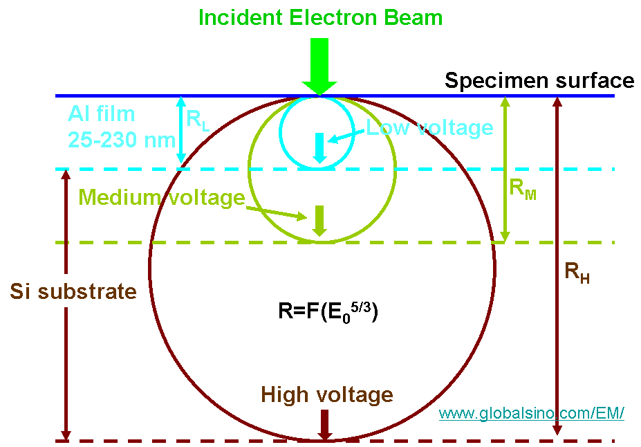
Figure 4835e. Schematic showing the maximum primary electron ranges RH, RM, and RL
with high, medium,
and low electron beam
voltages, respectively, for an Al thin film on Si wafer substrate specimen.
To know more about the dependence of the emission coefficient of secondary electrons on atomic number and accelerating voltage of incident electron beam, You need to refer to a discussion elsewhere. Furthermore, when the observing structure is electrically isolated, it can be charged during electron irradiation. When the charging process reaches an equilibrium state, the surface potential will maintain constant. In the case of positive charging, the surface potential VS is positive a few volts, retarding the part of the SEs at low-energies and resulting in a lower SE yield. On the other hand, in the case of negative charging, the negative surface potential slightly retards the incident primary electrons, while it increases the SE yield.
When the angle of incidence of the electron beam to a sample is increased, the secondary electron yield increases.
Table 4835. Secondary electron yield in EM. |
Beam energy |
0.25 keV |
0.5 keV |
1 keV |
2 keV |
5 keV |
10 keV |
15 keV |
30 keV |
60–300 keV |
| General |
|
|
|
|
|
|
|
|
a few % out of incident electrons |
| Al2O3 |
|
|
19 |
|
|
|
|
|
|
| MgO |
|
|
25 |
|
|
|
|
|
|
| NaCl |
|
|
17 |
|
|
|
|
|
|
| KCl |
|
|
16 |
|
|
|
|
|
|
| SiO2 |
|
4 |
|
|
|
|
|
|
|
| 1 |
H |
|
|
|
|
|
|
|
|
|
| 2 |
He |
|
|
|
|
|
|
|
|
|
| 3 |
Li |
|
|
|
|
|
|
|
|
|
| 4 |
Be |
|
|
|
|
|
|
|
|
|
| 5 |
B |
|
|
|
|
|
|
|
|
|
| 6 |
C |
1 |
0.45 |
|
|
|
|
|
|
|
| 7 |
N |
|
|
|
|
|
|
|
|
|
| 8 |
O |
|
|
|
|
|
|
|
|
|
| 9 |
F |
|
|
|
|
|
|
|
|
|
| 10 |
Ne |
|
|
|
|
|
|
|
|
|
| 11 |
Na |
|
|
|
|
|
|
|
|
|
| 12 |
Mg |
|
|
|
|
|
|
|
|
|
| 13 |
Al |
|
|
|
|
|
|
|
|
|
| 14 |
Si |
|
|
|
|
|
|
|
|
|
| 15 |
P |
|
|
|
|
|
|
|
|
|
| 16 |
S |
|
|
|
|
|
|
|
|
|
| 17 |
Cl |
|
|
|
|
|
|
|
|
|
| 18 |
Ar |
|
|
|
|
|
|
|
|
|
| 19 |
K |
|
|
|
|
|
|
|
|
|
| 20 |
Ca |
|
|
|
|
|
|
|
|
|
| 21 |
Sc |
|
|
|
|
|
|
|
|
|
| 22 |
Ti |
|
|
|
|
|
|
|
|
|
| 23 |
V |
|
|
|
|
|
|
|
|
|
| 24 |
Cr |
|
|
|
|
|
|
|
|
|
| 25 |
Mn |
|
|
|
|
|
|
|
|
|
| 26 |
Fe |
|
|
|
|
|
|
|
|
|
| 27 |
Co |
|
|
|
|
|
|
|
|
|
| 28 |
Ni |
|
|
|
|
|
|
|
|
|
| 29 |
Cu |
|
|
|
|
|
|
|
|
|
| 30 |
Zn |
|
|
|
|
|
|
|
|
|
| 31 |
Ga |
|
|
|
|
|
|
|
|
|
| 32 |
Ge |
|
|
|
|
|
|
|
|
|
| 33 |
As |
|
|
|
|
|
|
|
|
|
| 34 |
Se |
|
|
|
|
|
|
|
|
|
| 35 |
Br |
|
|
|
|
|
|
|
|
|
| 36 |
Kr |
|
|
|
|
|
|
|
|
|
| 37 |
Ru |
|
|
|
|
|
|
|
|
|
| 38 |
Sr |
|
|
|
|
|
|
|
|
|
| 39 |
Y |
|
|
|
|
|
|
|
|
|
| 40 |
Zr |
|
|
|
|
|
|
|
|
|
| 41 |
Nb |
|
|
|
|
|
|
|
|
|
| 42 |
Mo |
|
|
|
|
|
|
|
|
|
| 43 |
Tc |
|
|
|
|
|
|
|
|
|
| 44 |
Ru
|
|
|
|
|
|
|
|
|
|
| 45 |
Rh |
|
|
|
|
|
|
|
|
|
| 46 |
Pd |
|
|
|
|
|
|
|
|
|
| 47 |
Ag |
|
|
|
|
|
|
|
|
|
| 48 |
Cd |
|
|
|
|
|
|
|
|
|
| 49 |
In |
|
|
|
|
|
|
|
|
|
| 50 |
Sn |
|
|
|
|
|
|
|
|
|
| 51 |
Sb |
|
|
|
|
|
|
|
|
|
| 52 |
Te |
|
|
|
|
|
|
|
|
|
| 53 |
I |
|
|
|
|
|
|
|
|
|
| 54 |
Xe |
|
|
|
|
|
|
|
|
|
| 55 |
Cs |
|
|
|
|
|
|
|
|
|
| 56 |
Ba |
|
|
|
|
|
|
|
|
|
| 57 |
La |
|
|
|
|
|
|
|
|
|
| 58 |
Ce |
|
|
|
|
|
|
|
|
|
| 59 |
Pr |
|
|
|
|
|
|
|
|
|
| 60 |
Nd |
|
|
|
|
|
|
|
|
|
| 61 |
Pm |
|
|
|
|
|
|
|
|
|
| 62 |
Sm |
|
|
|
|
|
|
|
|
|
| 63 |
Eu |
|
|
|
|
|
|
|
|
|
| 64 |
Gd |
|
|
|
|
|
|
|
|
|
| 65 |
Tb |
|
|
|
|
|
|
|
|
|
| 66 |
Dy |
|
|
|
|
|
|
|
|
|
| 67 |
Ho |
|
|
|
|
|
|
|
|
|
68
|
Er |
|
|
|
|
|
|
|
|
|
69
|
Tm |
|
|
|
|
|
|
|
|
|
70
|
Yb |
|
|
|
|
|
|
|
|
|
71
|
Lu |
|
|
|
|
|
|
|
|
|
72
|
Hf |
|
|
|
|
|
|
|
|
|
73
|
Ta |
|
|
|
|
|
|
|
|
|
74
|
W |
|
|
|
|
|
|
|
|
|
75
|
Re |
|
|
|
|
|
|
|
|
|
76
|
Os |
|
|
|
|
|
|
|
|
|
77
|
Ir |
|
|
|
|
|
|
|
|
|
78
|
Pt |
|
|
|
|
|
|
|
|
|
79
|
Au |
|
|
|
|
|
|
|
|
|
80
|
Hg |
|
|
|
|
|
|
|
|
|
81
|
Tl |
|
|
|
|
|
|
|
|
|
82
|
Pb |
|
|
|
|
|
|
|
|
|
83
|
Bi |
|
|
|
|
|
|
|
|
|
84
|
Po |
|
|
|
|
|
|
|
|
|
85
|
At |
|
|
|
|
|
|
|
|
|
86
|
Rn |
|
|
|
|
|
|
|
|
|
87
|
Fr |
|
|
|
|
|
|
|
|
|
88
|
Ra |
|
|
|
|
|
|
|
|
|
89
|
Ac |
|
|
|
|
|
|
|
|
|
90
|
Th |
|
|
|
|
|
|
|
|
|
| 91 |
Pa |
|
|
|
|
|
|
|
|
|
| 92 |
U |
|
|
|
|
|
|
|
|
|
| Reference |
|
|
|
|
|
|
|
|
|
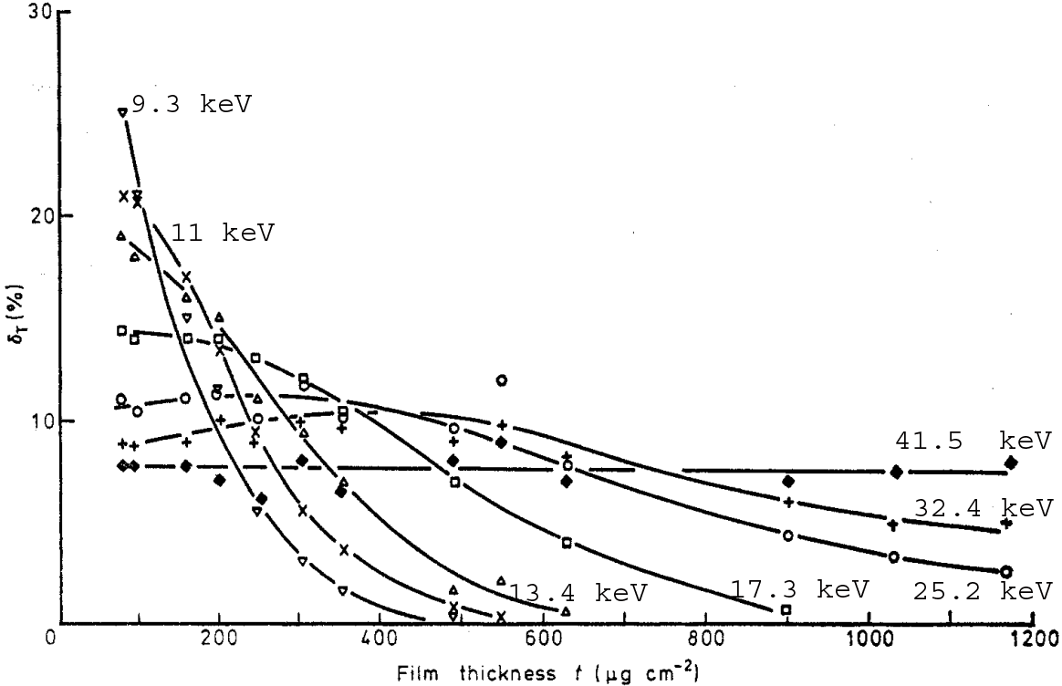
Secondary electron yield in TEM films
In general , more SEs are generated from the top surface than bottom surface of the TEM sample. (see page999)
For a TEM film sample, the secondary electron yield δT generated by the transmitted electrons from the bottom (exit) surface can be given by,
δT = δPE,TβTηT ----------------------------------- [4835b]
where,
ηT -- the transmission coefficient.
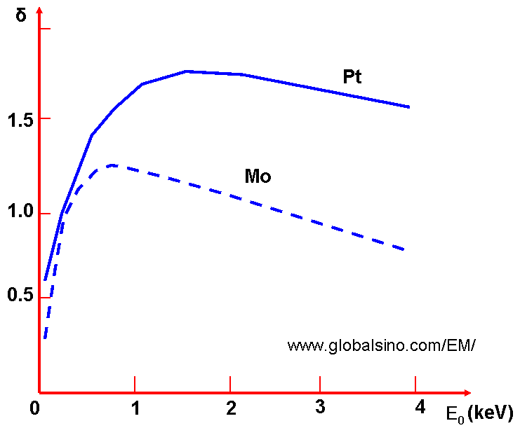
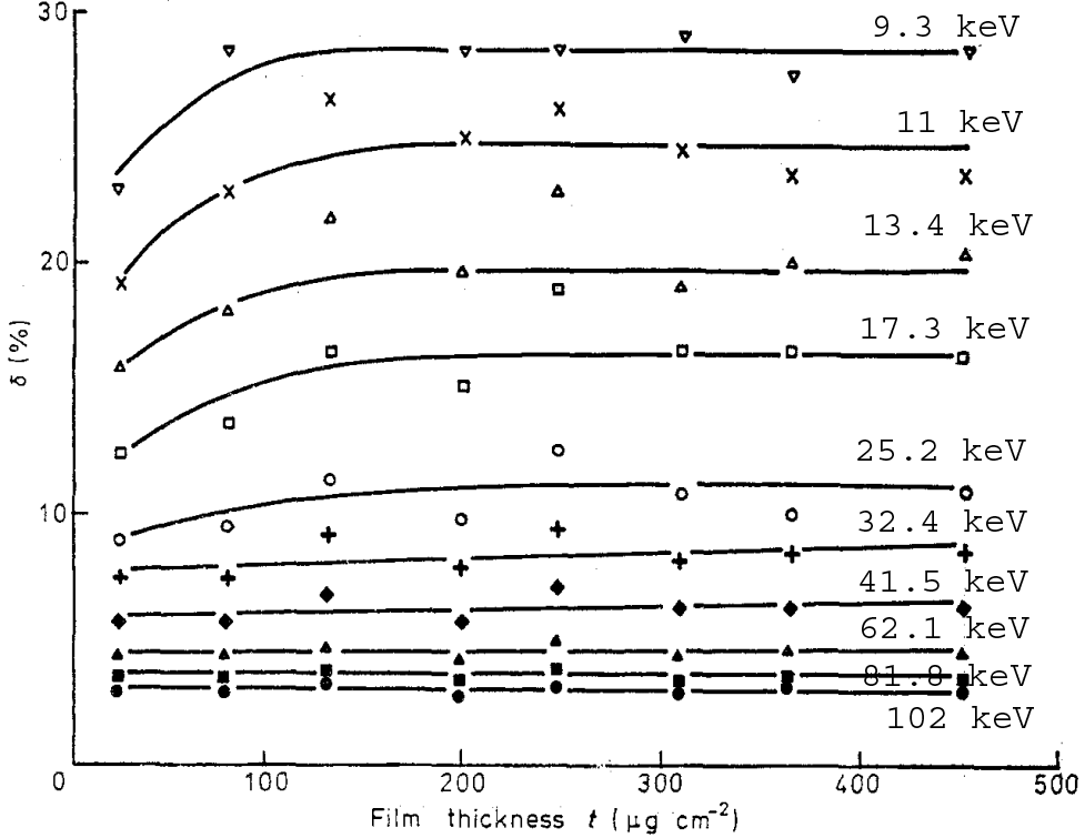
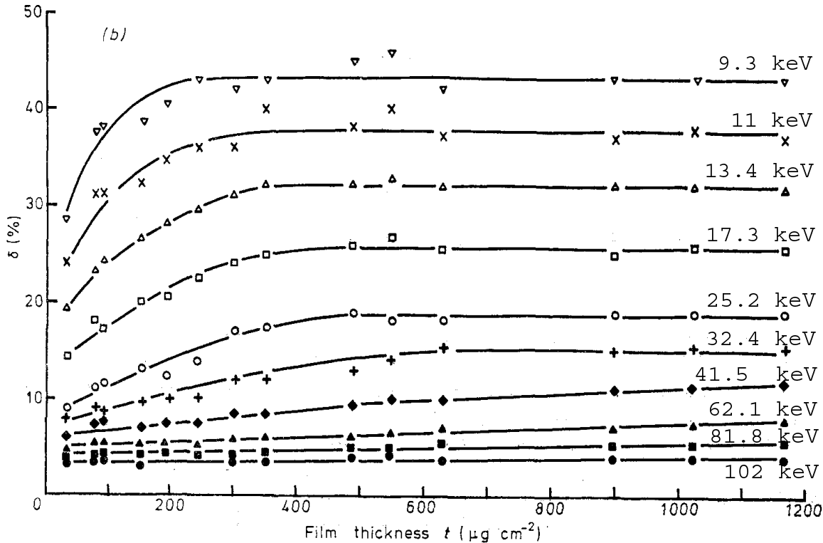
Figure 4835f shows the comparison between the secondary electron yields δ and δT generated by the incident and transmitted electrons on the top (entrance) surfaces and bottom (exit) surfaces, respectively, from Al and Au TEM films. The δ on the top surfaces of TEM samples, shown in Figure 4835f (a) and (c), increases with increasing film thickness, t, because the backscattering coefficient increases with thickness (see page4564).
| Figure 4835f. Secondary electron yields δ and δT generated by the incident and transmitted electrons on the top (entrance) surfaces and bottom (exit) surfaces, respectively, from Al and Au films: (a) δ for Al top surface, (b) δT for Al bottom surface, (c) δ for Au top surface, and (d) δT for Au bottom surface. Adapted from [9] |
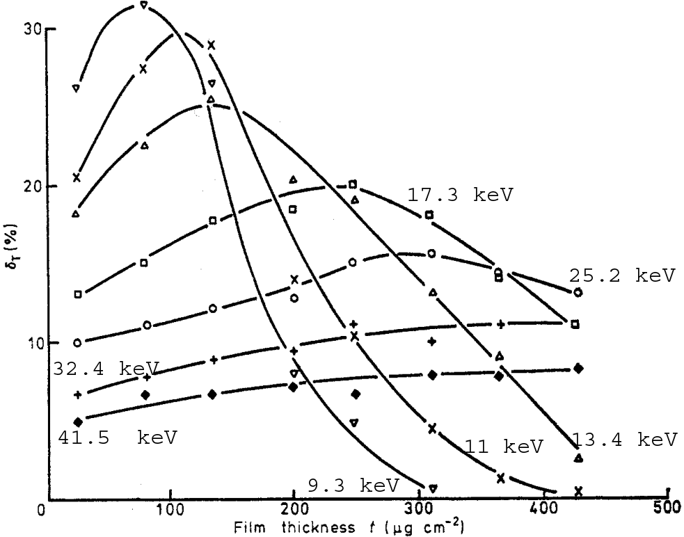
The dependence of SE yield δT, generated by the transmitted electrons from the bottom (exit) surface, on TEM sample thickness is:
i) The SE yield δT can increase at first with increasing film thickness, as shown in the Al cases in Figure 4835f (b), if the decrease of the energy of the transmitted electrons is significant and thus the interaction volume of the incident electron beam at the exit surface is dramatically modified.
ii) SE yield δT decreases with increasing TEM sample thickness due to the decrease in the number of transmitted electrons, as shown in Figure 4835g, because more incident electrons are backscattered in thicker TEM films and thus they cannot arrive at the exit surface. This is especially true in high voltage TEM measurements.
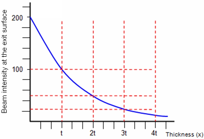
Figure 4835g. Beam intensity at the exit surface. |
[1] H. Salow, Zeit. Fuer Techni. Physik 21 (1940) 1.
[2] C.A.F. Pintȃo, R. Hessel, J. Appl. Phys. 88 (2000) 478.
[3] H. Seiler, J. Appl. Phys. 54 (1983) R1.
[4] D.C. Joy, J. Microsc. 147 (1987) 51.
[5] J. Cazaux, J. Phys. D: Appl. Phys. 38 (2005) 2433.
[6] H. Seiler, J. Appl. Phys. 54 (1983) R1.
[7] Dionne GF (1973) J Appl Phys 44(12):5361
[8] Lye RG, Dekker AJ (1957) Phys Rev 107(4):977
[9] L Reimer and H Drescher, Secondary electron emission of 10-100 keV electrons from transparent fdms of A1 and Au, J. Phys. D: Appl. Phys., Vol. 10, 1977.
|