Chapter/Index: Introduction | A | B | C | D | E | F | G | H | I | J | K | L | M | N | O | P | Q | R | S | T | U | V | W | X | Y | Z | Appendix
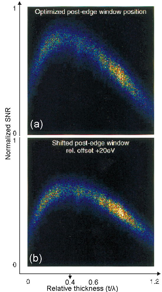
| In order to achieve good EELS and EFTEM results with well-resolved spectral signals, it is very important to prepare the TEM sample to have just the right range of thickness s in the interest area. The reason for this revolves around a parameter called the mean free path (λ) for inelastic scattering. This quantity depends on the elemental composition of the TEM sample as well as the beam energy and collection angle of the experiment, but a very rough, order of magnitude estimate of this parameter for typical materials at 200 keV beam energy is about 100 nm. A thin specimen can avoid multiple scattering which obscures the core-loss edges. That is, the sample should be so thin that the plasmon peak is smaller than one-tenth of the zero loss. Ideally, the interesting area for EFTEM or EELS analysis should have a thickness in the range of about 0.3 – 1.0 times λ. For many materials this means that sample thickness of about 50 – 70 nm are fairly ideal. Generally speaking, the background would increase faster than the characteristic signal with increasing specimen thickness [3], and because, consequently, the overall edge shape would be changed, it is essential to use thin or deconvoluted spectra only, to avoid plural scattering artifacts. For example, Figure 4995a shows two correlation plots of signal to noise ratio (SNR) of carbon EELS, calculated from filtered image series taken with a 25 eV slit at conditions in three window method: pre-edge 1 = 225 eV, pre-edge 2 = 265 eV and with post-edge = 295 eV and with energy window = 315 – 295 = 20 eV, respectively. The optimal specimen thickness is t/λ = ~0.4 for carbon under the condition of 200 keV (energy of the incident electron beam) and 7.6 mrad (collection angle). Extremely thin specimen areas cause the SNR to drop due to increased noise, whereas plural scattering in thick areas decreases the signal relative to the background. A shift of the post-edge window by 20 eV (Figure 4995a (b)) lowers the maximum SNR value of approximately 25% as a fact of a larger background extrapolation error (h) and a decreased signal.
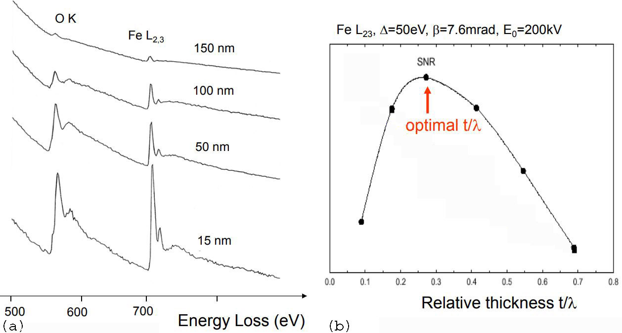
Figure 4995b shows the EELS of Fe2O3 material. One can see that the signal-to-noise ratio (SNR) of Fe L2,3 EELS signal is the highest at t/λ ≈ 0.3, namely t ≈34 nm.
[1] Optimization of the signal to noise ratio in EFTEM elemental maps with regard to different eonization edge types, Kothleitner, G and Hofer, F, Micron, 29, 5, pp. 349–357, (1998).
|