=================================================================================
In semiconductor, there is a big problem how to classify the wafer map pattern into serveral groups without manual action. The defect recognition of wafers can be performed by using the real-world wafer map dataset (WM-811K), provided by Taiwan Semiconductor Manufacturing
Company (TSMC) and built by Wu et al. [3]. Domain experts labeled some of these defect types on the wafers. The WM-811K is a dataset, which is the largest publicly available wafer map dataset to date and it can be downloaded from mirlab (Multimedia Information Retrieval Lab, Department of Computer Science,
National Taiwan University) [5, 23] or Kaggle [6]. The dataset is derived from the real
production process of wafers.
The dataset consists of wafer maps with
information about the wafer map, number of dies, lot name, wafer index in each lot, training or test set label and failure
pattern type, and only approximately 21% of the samples are labeled as shown in Figure 4236a and Table 4236a. Note that in research projects, the experiment is based on labeled
samples. The 811,457 images were collected from 811,457 wafers and 46,293 lots, in the data but only 172,950 images with manual label (totally 9 labels: 0、1、2、3、4、5、6、7、8) as shown in Figure 4236b. Only 172,950 wafers have actual wafer maps, whereas the rest were obtained by simulation. The 9 labels corresponds to nine different wafer patterns (Center, Donut, Edge-Location, Edge-Ring, Random,
Location, Near-Full, Scratch and None) as shown in Figure 4236c. Each pixel in the
image represents a die on wafer maps. Most
wafer maps are represented using a single channel grey-scale
image of size 256×256 pixels with 3 pixel levels: 0, 127 and 255 as binary wafer pass/fail
maps.
Locations with pixel level 0 are those
not part of the wafer. Grey pixels with pixel level 127 represent
die locations with a pass label while white pixels represent those
with a fail label. From the 172950 images, label:8 (none pattern) occupied 85.2%. The classification application with this real industry data is limited by the imbalanced distribution issue (some minority failure pattern types are dominated by other majority ones),
posing significant challenges for wafer defect classification models. The accuracy of wafer map classification with WM-811K can be as high as 96.63% in test set. [1]

| Figure 4236a. Visualization of dataset label. Around 630,000 of the data is
without the label, and 170,000 of the data is with the label. |
Table 4236a. Description of WM-811K dataset.
| Label |
Amount |
| Unlabeled |
Total |
638,570 |
| Labeled |
Total |
172,950 |
| None |
147,431 |
| Loc |
3,593 |
| Edge-Loc |
5,1589 |
| Edge-Ring |
9,680 |
| Center |
4,294 |
| Scratch |
1,193 |
| Random |
866 |
| Near-full |
149 |
| Donut |
555 |
| Total |
811,520 |

Figure 4236b. The structure of the WM-811K dataset.
[4]
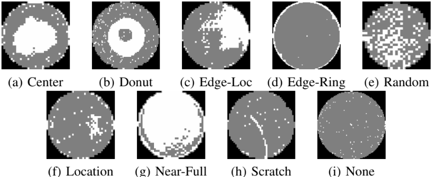
Figure 4236c. Sample wafer examples for different pattern types. [7]
Both Figures 4236d and 4236e show the failure type frequency of the WM-811K
dataset; however, they are not consistent.

Figure 4236d. Failure type frequency of WM-811K dataset. [16]

Figure 4236e. Wafer map distribution in the WM-811K dataset. [15]
In Figure 4236f, the column graph shows the
quantity distribution of labeled wafer maps in the WM-811K dataset. The samples are
divided according to the ratio of training set: validation set: test set = 60%:15%:25%). The
broken line shows the classification accuracy of ResNet-18 trained with the labeled data.
It can be seen the distribution is a long-tailed distribution: more header data (categories with large
sample sizes) and less tail data (categories with small sample sizes) [8]. Although the sample size of Near-Full pattern was small, the recognition rate was high.
While the sample sizes of Edge-Local and Local patterns were large, the recognition rates
were very low. According to the defect cluster characteristics, the researchers argued that the features of
Near-Full pattern are easy to identify and do not need large-scale sample training, while the
features of Edge-Local and Local patterns are difficult to distinguish. They proposed that this
is because the difficulty of feature recognition varies between classes. Therefore, it indicates that there are more necessary consideration to define this conjecture as the feature distribution imbalance between these eight defect patterns, and include it as one of
the perspectives to solve the dataset imbalance.

Figure 4236f. Distribution of the WM-811K dataset and classification accuracy of ResNet. [9]
Figure 4236g shows the image resolution distribution in the WM-811K dataset. The large samples are
concentrated inside a resolution length of 25–64 pixels on the x-axis and a resolution width of 25–71 pixels on the y-axis.

Figure 4236g. Image resolution distribution in the WM-811K dataset. [15]
By using the public dataset WM-811K, researchers achieved excellent classification performance. However, in these works, wafer monitoring is tackled as a closed-set classification problem, therefore these methods cannot detect novel defect
patterns. On the other hand, the WM-811K dataset only contains small images representing
Wafer Bin Maps.
Table 4236b. Some research related to the WM-811K dataset.
| Model |
Channel |
Resolution
size |
Training
samples |
Test
samples |
Overall
accuracy |
Reference |
| DCNN |
RBG |
[26, 26, 3] |
12730 |
705 |
99.29% |
[16] |
| PCACAE |
Grayscale |
[96, 96, 1] |
13451 |
4483 |
97.27% |
[17] |
| GAN-CNN |
Grayscale |
[64, 64, 1] |
8160 |
1000 |
98.30% |
[18] |
| CNN-ECOC-SVM |
Grayscale |
[256, 256, 1] |
18000 |
2000 |
98.43% |
[19] |
| DMC1 |
RBG |
[64, 64, 3] |
103770 |
51885 |
97.01% |
[20] |
| VGG-19 |
Grayscale |
[96, 96, 1] |
11760 |
9471 |
84.81% |
[21] |
| ResNet-34 |
Grayscale |
[96, 96, 1] |
11760 |
9471 |
81.91% |
[21] |
| ResNet-50 |
Grayscale |
[96, 96, 1] |
11760 |
9471 |
87.84% |
[21] |
| MobileNetV2 |
Grayscale |
[96, 96, 1] |
11760 |
9471 |
85.39% |
[21] |
| T-DenseNet |
Grayscale |
[224, 224, 1] |
7112 |
2000 |
87.70% |
[22] |
Although the WM-811K dataset has already been divided into the training and testing sets by experts, some researchers have applied their additional considerations into the application of the dataset due to different reasons:
i) Gong and Lin [7] had not
followed the existing data separation from the dataset but defined their own training and test datasets. They claimed that ideally each of the 47543 lots
should have 25 wafer maps, leading to 1,157,325 total wafer maps. However, in reality, some wafer maps were somehow
missing in some lots. On the other hand, according to the failure type information analysis in the dataset, only 25519 wafer maps
had real defect patterns, while 147431 wafers had no defect patterns (labeled “none”) and 638507 wafers had no
labels. Since they are only interested in wafers with real failure patterns, they had removed the vast majority of the wafer maps
and only those 25,519 samples are useful in their study.
Furthermore, the dimensions of the wafer maps in the dataset were not uniform. Based on the waferMap column
information (“0”, “1” and “2” represent the regions with no die, a normal die and a defective die respectively) from
the dataset, the wafer map dimensions could then be extracted and turn out to be not the same size. Therefore, data normalization was
first performed via dividing this waferMap column data by 2, which converted the data type from int to float and
therefore made the resizing process possible. In order to minimize the upsizing and downsizing errors after the image
size unification, they calculated the weighted average dimensions of the 25519 wafer maps in the x and y directions
and found that the optimal dimensions should be chosen as 42 × 42 . The resizing errors during data
transformation can potentially serve as regularization.
They also mentioned that the other big issue for this dataset was its highly imbalanced data distribution among the 8 failure pattern types. Then, they
applied two data augmentation strategies to solve this data imbalance problem, namely flipping and rotating.
As for the data split, they used two different approaches.
ii) Jo and Lee [10] split the data into training, validation, and test data as shown in Table 4236c. There is only none
type data in the training set and 80% of all none type data. There is 10% of all
none type data in the validation set, and there are other patterns with 50% of
all each pattern. On the other hand, the rest of the datasets were used as test sets.
Table 4236c. Number of experiment data from WM-811K.
| Failure Type |
Train |
Validation |
Test |
| None |
117,944 |
14,743 |
14,744 |
| Loc |
0 |
1,796 |
1,797 |
| Edge-Loc |
0 |
2,594 |
2,595 |
| Edge-Ring |
0 |
4,840 |
4,840 |
| Center |
0 |
2,147 |
2,147 |
| Scratch |
0 |
596 |
597 |
| Random |
0 |
433 |
433 |
| Near-full |
0 |
74 |
75 |
| Donut |
0 |
277 |
278 |
| Total |
117,944 |
27500 |
27506 |
iii) In the wafer pattern classification with WM-811K done by Yunseon Byun and Jun-Geol Baek, [11] each pixel in the
images represented a die on wafer maps. After testing, the
normal chip was represented as 1, and the defective chip
was represented as 2. Although the shape of the wafer was
a circle, the inputs of the convolutional neural network had to be square. Therefore, the empty pixel was represented as
0. The goal of the experiment was to classify the
defective patterns. Since the size of all images is not the same and most of them are rectangular, they resized the data
to the 26 x 26 square images for the training of CNNs. They used only 7,915 to train the model, and the
data is divided into 7:3 and used for training and testing. In their study, the recognition of mixed-type
defect patterns requires the mixed-type data on wafer
maps. They generated the mixed-type patterns through
the computation of single-type patterns. The target
patterns for generation are center, scratch, edge-loc,
and edge-ring patterns. In their study, only two
single-type patterns can be mixed. Then, the generated
patterns are the mixture of edge-loc and scratch, the mixture of edge-loc and center, the mixture of edge-ring and scratch, the mixture of edge-ring and center, and the mixture of scratch and center as shown in
Figure 4236h.

Figure 4236h. Mixed-type defect pattern maps. [11]
iv) To balance the training data, Cha and Jeong [12] randomly extracted 400 from each class. Then, they increased the amount of data by data augmentation to improve the performance of the model.
v) Hu et al. [13]
used 54,355 labeled wafer maps in the dataset, and split them
into a training dataset and a testing dataset with a percentage of
90% and 10%, respectively. In order to perform the proposed
semi-supervised contrastive learning framework, all the 48920
wafer maps in the training dataset were used to construct the
unlabeled dataset DU. Only a small portion pd% of the training
dataset was collected to build the labeled dataset DL, containing
both wafer maps and the corresponding patterns, which was
applied for both the proposed semi-supervised learning method
and the supervised learning methods for comparison.
Table 4236d. WM-811K dataset statistics.
| Wafer map patterns |
Training |
Testing |
| None |
33051 |
3679 |
| Center |
3113 |
349 |
| Donut |
372 |
37 |
| Edge-Loc |
2150 |
267 |
| Edge-Ring |
7735 |
819 |
| Loc |
1458 |
162 |
| Random |
546 |
63 |
| Scratch |
446 |
54 |
| Near-full |
49 |
5 |
| Total |
48920 |
5435 |
vi) Due to the uneven class quantity and image size, Yang and Yu [14] randomly sampled 3150 images from seven classes and resize them into 32 x 32. For the augmentation strategy, they applied horizontal flipping, vertical flip-ping, and rotation in WM-811K.
vii) The
highest and lowest percentage distributions of these eight defect types in WM-811K maps are local and donut failure types and the percentage
difference is about 0.37%. Wang et al. [15] stated that data imbalance is a crucial problem, and it needs to be trained to train a good DL model for pattern recognition of wafer maps. Thus, proper data balancing techniques are required to achieve good classification performance.
viii) In the study of Wang et al., [15] the original WM-811K data set had been preprocessed to identify labeled and unlabeled patterns, and then the class distribution of the labeled patterns was checked. The image size of the original data
set was then adjusted to the required resolution to see the impact of different image resolutions on the model’s classification performance.
ix) Figure 4236i shows the number of each failure pattern (None pattern as an exception). The distribution of each type is imbalanced. In order to take into account the different die size, each record of raw data of a wafer map is transformed into an
image with 300×300 pixels.

| Figure 4236i. Count of wafer maps for
experiments (Training: 64%,
Validation: 16%, Testing: 20%). [24] |
x) Researcher [2] split 25519 images into 15316(60%) train、3823(15%) validation and 6380(25%) test and use test data sets to varified his model:
train : 15316(60%):
Center : 2598(17.0%)
Donut : 326(2.1%)
Edge-Loc : 3081(20.1%)
Edge-Ring : 5873(38.3%)
Loc : 2106(13.8%)
Random : 516(3.4%)
Scratch : 719(4.7%)
Near-full : 97(0.6%)
validation : 3823(15%):
Center : 640(16.7%)
Donut : 78(2.0%)
Edge-Loc : 779(20.4%)
Edge-Ring : 1426(37.3%)
Loc : 571(14.9%)
Random : 124(3.2%)
Scratch : 186(4.9%)
Near-full : 19(0.5%)
test : 6380(25%):
Center : 1056(16.6%)
Donut : 151(2.4%)
Edge-Loc : 1329(20.8%)
Edge-Ring : 2381(37.3%)
Loc : 916(14.4%)
Random : 226(3.5%)
Scratch : 288(4.5%)
Near-full : 33(0.5%)
Example of training and testing of the model were carried out on a DELL
T7920 workstation (Round Rock, Texas, USA).
[9] The main hardware configuration was twoGeForce RTX 2080TI graphics cards and a 64 GB memory. The software environment isUbuntu 18.04 and was implemented based on the PyTorch deep learning framework. The
cross-entropy loss was used for model training, and the initial learning rate was set at 0.01,
which was reduced by a factor of ten when the number of iterations reached half of the
total number. In the representation learning stage, ResNet-18 integrated with the improved
CBAM algorithm was trained for 100 epochs. In the classifier fine-tuning stage, the model based on the previous stage was fine-tuned for 25 epochs at a learning rate of 0.001.
============================================
Unpack the LSWMD.pkl and then read and/or save single image(s). code:
Output:


When the line in the code is changed to:

Then, the output becomes:

============================================
Heatmap with input from a csv/pkl file. (page4277)
============================================
Display the labeled features and a specific pattern. code:

Output:


============================================
Full execution of wafer identification with Convolutional autoencoder (CAE), VGG-16 Model, GAP(Global Average Pooling) and VGG-16 (To complete the program execution, 15 hours are needed). code and output:


============================================
Remove rows in DataFrame under certain conditions. code:

Input:


Output:


============================================
Extract images with different features into different pkl files. code:


Input:
Output:


============================================
Extract maps from a subfile of the LSWM database. code:

Input:


[1] Tsung-Han Tsai and Yu-Chen Lee, Wafer Map Defect Classification with Depthwise Separable Convolutions, IEEE International Conference on Consumer Electronics (ICCE), DOI: 10.1109/ICCE46568.2020.9043041, 2020.
[2] https://github.com/fr407041/WM-811K_semiconductor_wafer_map_pattern_classified.
[3] M.-J. Wu, J.-S. R. Jang, and J.-L. Chen, “Wafer map failure pattern
recognition and similarity ranking for large-scale data sets,” IEEE Trans.
Semicond. Manuf., vol. 28, no. 1, pp. 1–12, Feb. 2015.
[4] Tsung-Han Tsai and Yu-Chen Lee, Wafer Map Defect Classification with Depthwise Separable Convolutions, IEEE International Conference on Consumer Electronics (ICCE), DOI: 10.1109/ICCE46568.2020.9043041, 2020.
[5] WM811K Mirlab.org. (2018). MIR Corpora. Accessed: Apr. 7, 2018.
[Online].Available: http://mirlab.org/dataSet/public/.
[6] https://www.kaggle.com/datasets/qingyi/wm811k-wafer-map.
[7] Jie Gong and Chen Lin, Wafer Map Failure Pattern Classification Using Deep Learning, 2019.
[8]
Reed, W.J. The Pareto, Zipf and other power laws. Econ. Lett. 2001, 74, 15–19.
[9] Qiao Xu, Naigong Yu and Firdaous Essaf, Improved Wafer Map Inspection Using Attention Mechanism and Cosine Normalization, Machines, https://doi.org/10.3390/machines10020146, 10, 146, 2022.
[10] Ha Young Jo and Seong-Whan Lee, One-Class Classification for Wafer Map using Adversarial Autoencoder with DSVDD Prior, https://doi.org/10.48550/arXiv.2107.08823, Machine Learning, 2021.
[11] Yunseon Byun and Jun-Geol Baek, Mixed Pattern Recognition Methodology on Wafer Maps with Pre-trained Convolutional Neural Networks, 2022.
[12] Jaegyeong Cha and Jongpil Jeong, Improved U-Net with Residual Attention Block for Mixed-Defect Wafer Maps, Applied Sciences, https://doi.org/10.3390/app12042209, 2022.
[13] Hanbin Hu, Chen He and Peng Li, Semi-supervised Wafer Map Pattern Recognition using Domain-Specific Data Augmentation and Contrastive Learning, DOI: 10.1109/ITC50571.2021.00019, 2021 IEEE International Test Conference (ITC), 2021.
[14] Song-Bo Yang and Tian-li Yu, Pseudo-Representation Labeling Semi-Supervised Learning, https://doi.org/10.48550/arXiv.2006.00429, 2020.
[15] Fu-Kwun Wang, Jia-Hong Chou, Zemenu Endalamaw Amogne, A Deep convolutional neural network with residual blocks for wafer map defect pattern recognition, https://doi.org/10.1002/qre.2983, 2021.
[16] Ashadullah Shawon, Md Omar Faruk, Masrur Bin Habib, Abdullah Mohammad Khan, Silicon Wafer Map Defect Classification Using Deep Convolutional Neural Network With Data Augmentation, 2019 IEEE 5th International Conference on Computer and Communications (ICCC 2019).
[17] Yu J, Liu J. Two-dimensional principal component analysis-based convolutional autoencoder for wafer map defect detection. IEEE Trans
Ind Electron. 2021;68(9):8789-8797.
[18] Ji Y, Lee JH, Using GAN to improve CNN performance of wafer map defect type classification: yield enhancement. In: 2020 31st Annual
SEMI Advanced Semiconductor Manufacturing Conference (ASMC). Saratoga Springs, NY, USA, 2020:1-6.
[19] Jin CH, Kim HJ, Piao Y, Li M, Piao M. Wafer map defect pattern classification based on convolutional neural network features and error-
correcting output codes. J Intell Manuf. 2020;31(8):1861-1875.
[20] Tsai TH, Lee YC. A light-weight neural network for wafer map classification based on data augmentation. IEEE Trans Semicond Manuf.
2020;33(4):663-672.
[21] Maksim K, Kirill B, Eduard Z, et al. classification of wafer maps defect based on deep learning methods with small amount of data. In:
2019 International Conference on Engineering and Telecommunication (EnT). Dolgoprudny, Russia, 2019:1-5.
[22] Shen Z, Yu J, Wafer map defect recognition based on deep transfer learning. In: 2019 IEEE International Conference on Industrial Engineering and Engineering Management (IEEM). Macao, China, 2019:1568-1572.
[23] Multimedia Information Retrieval Lab Data Set Department of Computer Science National
Taiwan University Retreived From http://mirlab.org/dataSet/public/.
[24] Chia-Yu Hsu and Ju-Chien Chien, Ensemble convolutional neural networks with weighted majority for wafer bin map pattern classification, Journal of Intelligent Manufacturing, https://doi.org/10.1007/s10845-020-01687-7, 2020.
|
