Short Fail in DRAM - Integrated Circuits and Materials - - An Online Book - |
||||||||
| Python for Integrated Circuits http://www.globalsino.com/ICsAndMaterials/ | ||||||||
| ================================================================================= | ||||||||
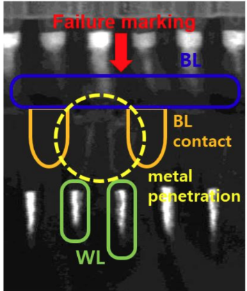
Short failure in DRAM is often caused by misalignment of isolation layer or mask contamination. [1] Bridge that are caused by extra metal deposition or isolation breakdown. Bridge defects can occur between BL (Bit Line) contact and BCAT (Buried Cell Array Transistor), caused by isolation breaking. [2] Figure 2015a (b) shows that cross bridge defects between BL and WL are induced by the lack of metal etch back (MEB) or poly etch back (PEB) of BCAT caused by various particle. [1] Due to the particle, silicon-nitride (SiN) is not filled on the BCAT material, which caused a short fail. Such defects are mainly observed in the first test step and initially appears as column failure. In this situation, if WL located in failure marking is turned on, VBL goes high level due to charge sharing and sensing operation because high level of WL and BL are electrically connected. On the other hand, if adjacent WL in failure marking is turned off, BL goes low level because of low level of WL. Figure 2015a (c) shows extended cross-defects that there are complex mutual reactions between defects such as both WL and BL failure. It can cause errors at the system level with a very high probability even though there is ECC. The extended cross-defects accompanied by two WL defects have been frequently found as shown in Figure 2015b, where the particle exists in the BL contact area.
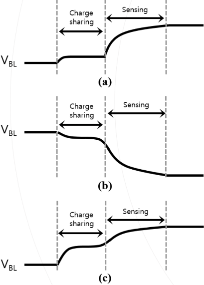
Figure 2015c shows timing diagram for data-1 read operation related to VBL. Figure 2015c (a) illustrates a level of normal BL for data-1. Figure 2015c (b) shows the case of data-1 read operation with defective adjacent WL turned on. Figure 2015c (c) shows the case of defective WL turned on. The fact that defective adjacent WL is turned on means that failure WL level is low. Therefore, the VBL drops significantly from charge sharing to sensing due to connection with low WL level even if cell charge is high. On the other hand, if defective WL turns on, failure WL level is high. Thus, VBL level goes up with help from charge sharing to sensing due to connection with high level of WL.
[1] Jaehoon Lee, Jinseon Kim, Dongguk Han, Seunghun Lee, Sunwoo Kim, Jingyeong Seol, Seungjin Lee, Kyoungrak Cho, Incheol Nam, Daesun Kim, Beomseop Lee, Heeil Hong, and Sangjun Hwang, A Failure Caused by Extended Cross-Defect in DRAM, ISTFA 2023: Proceedings of the 49th International Symposium for Testing and Failure Analysis Conference November 12—16, 2023, Phoenix, Arizona, USA https://doi.org/10.31339/asm.cp.istfa2023p0187. |
||||||||
| ================================================================================= | ||||||||
|
|
||||||||